s Overview
The AN6780 and AN6780S are ICs designed for general pur-
pose long interval timers. They consists of an oscillator, fre-
quency divider (flip-flop 15steps), output circuit, and power
circuit. A cycle can be freely set with the external resistor (R
T
)
and capacity (C
T
) of the oscillator.
s Features
∑
High inflow and outflow current : I
O
=±15mA max
∑
Small variation of oscillations
∑
Long interval timer setting : max 1 week
s Applications
Timers, integrating timers, superlow frequency oscillators
AN6780, AN6780S
General Purpose Long Interval Timers
7
6
5
4
3
2
1
0.3
+ 0.1
≠ 0.05
18.2
±
0.3
6.0
±
0.3
2.4
±
0.25
1.5
±
0.25
0.5
±
0.1
2.54
1.5
±
0.25
3.0
±
0.3
Unit : mm
AN6780
3.5
±
0.25
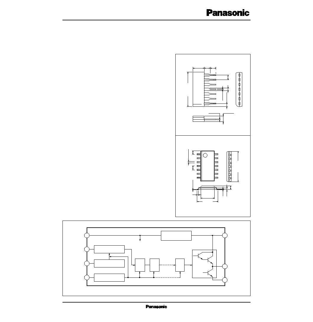
7-pin SIL Plastic Package (SIP007-P-0000)
1
5
2
3
7
6
4
Voltage Stabilizer
To each block
Input Circuit
Input Circuit
Oscillator
The pin numbers in ( ) are for the AN6780S.
Output
Circuit
F/F
15
F/F
2
F/F
1
(2)
(9)
(4)
(6)
V
CC
(12)
(11)
(8)
GND
s Block Diagram
Unit : mm
AN6780S
1.24
0.4
±
0.25
1.27
0.1
±
0.1
0.3
1.5
±
0.2
0.65
0.15
1
2
3
4
5
6
7
14
13
12
11
10
9
8
6.5
±
0.3
4.2
±
0.3
14-pin PANAFLAT Plastic Package (SOP014-P-0225A)
10.1
±
0.3
V
CC
V
1≠4 (2≠8)
V
2, 3≠4 (4, 6≠8)
V
5≠4 (9≠8)
V
6≠4 (11≠8)
I
CC
I
6 (11)
P
D
T
opr
T
stg
V
V
V
V
V
mA
mA
mW
∞C
∞C
Parameter
Symbol
Rating
Unit
s Absolute Maximum Ratings (Ta=25∞C)
13
V
CC
*
1
30
360
≠20 to +75
≠55 to +125
0
0
0
≠15
4
13
4
15
Voltage
Current
Power dissipation
Temperature
Supply voltage
Circuit voltage
Supply current
Circuit current
Operating ambient temperature
Storage temperature
*1 When output is at "H", the pin number are for the AN6780S
Parameter
Symbol
Range
s Recommended Operating Range (Ta=25∞C)
Operating supply voltage range
V
CC
4.5V to 12V
Parameter
Symbol
Condition
min
typ
max
s Electrical Characteristics (Ta=25∞C)
Supply current
I
CC
10
mA
6.5
V
CC
=12V
Oscillator charging current
I
1
(I
2
)
mA
0.3
V
CC
=5V, R=10k
Input current high level
I
IH
10
µ
A
V
CC
=12V, V
IH
=12V
Input current low level
I
IL
µ
A
V
CC
=4.5V, V
IL
=0V
Output voltage high level
V
OH1
V
V
CC
=5V, I
OH
=≠1mA
V
V
CC
=9V, I
OH
=≠10mA
Output voltage high level
V
OH2
V
V
CC
=5V, I
OL
=10mA
Output voltage low level
V
OL1
V
V
CC
=9V, I
OL
=10mA
Output voltage low level
V
OL2
V
Input voltage high level
V
IH
V
Input voltage low level
V
IL
0.8
0.4
500
0.35
0.4
2
4
0.26
3
5
Unit
s Pin Descriptions
AN6780
Pin No.
Description
Symbol
1
2
3
4
5
6
7
AN6780S
2
4
6
8
9
11
12
V
S
Stop
Reset
GND
CR
Output
V
CC
Internal stabilized power supply
Oscillation stop input
Reset input
Ground
C.R. connection
Output
Supply voltage
AN6780S : The Pins1, 3, 5, 7,10, 13 and 14 are non-contact.

(2)
1
(4)
2
(6)
3
(8)
4
V
CC
Pins numbers in ( )
are for the AN6780S
Oscillation interval T
O (S)
0.69R
T
(
) ∑ C
T
(F)
Output interval T
I (S)
22R
T
(k
) ∑ C
T
(
µ
F)
Integrating timer interval
T
S (s)
11R
T
(k
) ∑ C
T
(
µ
F) + (T
1
+ T
2
+ ∑∑∑)
Timer interval T
t (S)
11R
T
(k
) ∑ C
T
(
µ
F)
R
T
1 to 10
µ
F
C
T
R
L
V
CR
Output
T
O
T
1
= 32768T
O
(9)
5
AN6780, AN6780S
(11)
6
(12)
7
≠
+
V
CC
Pin numbers in ( ) are for the AN6780S
Reset
(Timer control)
R
T
1 to 10
µ
F
C
T
R
L
AN6780, AN6780S
≠
+
V
CR
Reset
T
O
T
S
= T
1
+ T
2
+ 16384T
O
Stop
Output
T
1
T
2
V
CR
Output
Reset
T
O
V
CC
R
T
Pin numbers in ( ) are for the AN6780S
1 to
10
µ
F
C
T
R
L
AN6780, AN6780S
≠
+
T
t
=16384T
O
T
t
1) Superlow frequency oscillator
2) Timer
3) Integrating timer
Integration input
(2)
1
(4)
2
(6)
3
(8)
4
(9)
5
(11)
6
(12)
7
(2)
1
(4)
2
(6)
3
(8)
4
(9)
5
(11)
6
(12)
7
s Application Circuit
6
The pin numbers in ( ) are for the AN6780S
(11)
Obeserve the following in order to prevent destruction
and reliability of the IC during its use.
1) For distribution of the oscillation frequency, take about
17% (IC alone) into account at the time of designing.
When accuracy is requested, use a variable resistor as a
timed resistor to make adjustment.
2) For the timed resistor, use a polyester capacitor with low
tan
, whose resistance is 1k
to 1M
and timed capacity
of 0.1
µ
F.
3) The values obtained from the timer interval calcuation
expression, etc. in Application Circuit change depending
on accuracy of the timed capacity in the actual set, etc.
4) Attach a capacity (1 to 10
µ
F) to the Pin1 (2) in order to
protect the IC against noises and stabilize its operation.
5) During normal operation, when you turn on the power
after extremely short period of power-off, note that auto
reset may not be applied due to residual potential of
external capacity.
6) Take a proper countermeasure noises in order to prevent
malfunctioning from being caused by external noises.
Particularly, when setting a long interval, pay attention to
the external noises.
7) When a plunger or relay is connected to the output circuit,
connect diodes to both ends of the coil in order to protect
the IC against counter electromotive power generated
after power-off
s Supplementary Descriptions
∑ Precautions on Use

1
2
3
Mode
L
H
H
Reset
*
H
L
Stop
Stop
Start
Stop
Oscillator
Clear
Counting
Stop Holds the previous state
Frequency divider
H
Counting
Stop Holds the previous state
Output
∑ Truth Table (Positive Logic)
Note) *Either L or H will do. When the power is turned on, control proceeds to the mode 2 or mode 3 from the mode 1, depending
on the reset/stop input state.
10
5
10
4
10
3
10
2
10
1
10
≠1
10
≠2
Timed Resistance R
T
(k
)
Oscillation Frequency f
OSC
(Hz)
f
OSC
≠ R
T
C
T
=0.1
µ
F
1
µ
F
10
µ
F
100
µ
F
1
16
12
8
4
0
High Output Current I
OH
(mA)
High Output Voltage V
OH
(V)
V
OH
≠ I
OH
0
4
8
12
16
20
10
10
2
10
3
10
6
10
5
10
4
10
3
10
2
10
1
Timed Resistance R
T
(k
)
Timer Interval T
t
(s)
T
t
≠ R
T
1
200
160
120
80
40
0
Low Output Current I
OL
(mA)
Output Voltage V
OL
(mV)
V
OL
≠ I
OL
10
10
3
0
4
8
12
16
20
10
2
C
T
=100
µ
F
10
µ
F
1
µ
F
0.1
µ
F
1week
1day
10hrs.
60min.
10min.
1min.
Ta=25∞C
10
9
8
7
6
5
4
3
2
1
0
Supply Voltage V
CC
(V)
Supply Current I
CC
(mA)
I
CC
≠V
CC
0
Ta=25∞C
Ta=25∞C
1.02
1.01
1.00
0.99
0.98
Ambient Temperature Ta (∞C)
Nomalized Oscillation f
OSC
(14.5kHz)
f
OSC
≠ Ta
≠40
0
40
80
120
V
CC
=5V
C
T
=0.1
µ
F
R
T
=1k
12V
V
CC
=5V
V
CC
=12V
9V
5V
2
4
6
8
10
12
14
16
T
t
s Characteristics Curve