 | –≠–ª–µ–∫—Ç—Ä–æ–Ω–Ω—ã–π –∫–æ–º–ø–æ–Ω–µ–Ω—Ç: AN7198Z | –°–∫–∞—á–∞—Ç—å:  PDF PDF  ZIP ZIP |

ICs for Audio Common Use
1
AN7198Z
Dual 20 W BTL Power IC for Car Audio
s
Overview
The AN7198Z is an audio power IC developed for the
sound output of car audio (Dual 20 W).
A capacitor and a resistor between the output pin and
GND to stop oscillation are built-in so that a space saving
of set is possible. Also, it is incorporates an industry's
first superior muting circuit which is free from shock
noise, so that a shock noise design under the set transient
condition can be made easily when the muting circuit is
used together with its standby function.
In addition, it is incorporating various protective cir-
cuits to protect the IC from destruction by GND-open
short circuit to GND and power supply surge which are
the important subjects of power IC protection, and the IC
will largely contribute to a high reliability design of equip-
ment.
s
Features
∑
Built-in various protection circuits (Realizing high breakdown voltage against destruction)
Power supply surge breakdown voltage of 80 V or more
Ground-open breakdown voltage of 16 V or more
∑
Built-in standby function (Free from shock noise at STB-on/off)
∑
Built-in muting function
Free from shock noise at mute-on/off
Adapting attenuator method, so that abnormal sound due to waveform deformation is not generated
Attack time, recovery time of 50 ms or less
∑
Reduction in external components
No capacitors and resistors for oscillation stop are unnecessary
It eliminates the need for NF and BS electrolytic capacitors
Muting function is unnecessary
Power supply choke coil is unnecessary
∑
Provided with beep sound input pin
∑
High sound quality design
s
Applications
∑
Car audio
HZIP015-P-0745A
18.00±0.30
13.50±0.30
3.60±0.10
10.0±0.30
1
15
4.00±0.20
1.50±0.10
0.50
+0.20
≠0.10
(0.61)
(2.54)
0.25
+0.15
≠0.05
R0.55
3.25±0.10
13.25±0.30
18.95±0.50
15.65±0.50
1.27
(1.80)
(1.95)
19.00±0.30
19.30±0.30
2.40±0.50
Unit: mm

AN7198Z
ICs for Audio Common Use
2
s
Pin Description
s
Absolute Maximum Ratings
Parameter
Symbol
Ratings
Unit
Supply voltage
*2
V
CC
25
V
Peak supply voltage
*3
V
surge
60
V
Supply current
I
CC
9.0
A
Power dissipation
*4
P
D
59
W
Operating ambient temperature
*1
T
opr
-
30 to
+
85
∞
C
Storage temperature
*1
T
stg
-
55 to
+
150
∞
C
Note) *1: T
a
=
25
∞
C except operating ambient temperature and storage temperature.
*2: Without signal
*3: Time
=
0.2 s
*4: T
a
=
85
∞
C
s
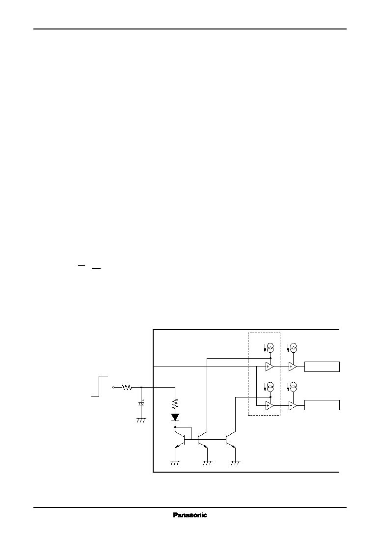
Block Diagram
Pin No.
Description
1
Power supply
2
Ch.1 output (
+
)
3
Grounding (output ch.1)
4
Ch.1 output (
-
)
5
Standby
6
Ch.1 input
7
Muting
8
Grounding (board)
Pin No.
Description
9
Grounding (input)
10
Beep sound input
11
Ch.2 input
12
Ripple filter
13
Ch.2 output (
-
)
14
Grounding (output ch.2)
15
Ch.2 output (
+
)
Ref.
Protection Cct.
Att.Con.
Att
Att
Att
Att
3
4
2
14
13
12
1
V
CC
8
GND(Sub)
GND (Input)
Beep In
ch.1 In
ch.2 In
Ripple Filter
Standby
Mute
10
6
5
7
11
9
15
ch.1 GND
ch.2 GND
ch.1 Out (
-
)
ch.1 Out (
+
)
ch.2 Out (
-
)
ch.2 Out (
+
)

ICs for Audio Common Use
AN7198Z
3
s
Electrical Characteristics at V
CC
=
13.2 V, f
=
1 kHz, T
a
=
25
∞
C
Parameter
Symbol
Conditions
Min
Typ
Max
Unit
Quiescent current
I
CQ
V
IN
=
0 mV, R
L
=
4
150
250
mA
Standby current
I
STB
V
IN
=
0 mV, R
L
=
4
1
10
µ
A
Output noise voltage
*1
V
NO
R
g
=
10 k
, R
L
=
4
0.18
0.5
mV[rms]
Voltage gain 1
G
V1
V
IN
=
40 mV, R
L
=
4
32
34
36
dB
Total harmonic distortion 1
THD
1
V
IN
=
40 mV, R
L
=
4
0.05
0.4
%
Maximum output power 1
P
O1
THD
=
10
%
, R
L
=
4
16
18.5
W
V
CC
=
14.4 V, R
L
=
4
22.0
W
Ripple rejection ratio
*1
RR
R
L
=
4
, R
g
=
10 k
, V
r
=
1 V[rms]
60
65
dB
f
r
=
1 kHz
Channel balance
CB
V
IN
=
40 mV, R
L
=
4
0
1
dB
Cross-talk
*1
CT
V
IN
=
40 mV, R
L
=
4
, R
g
=
10 k
60
79
dB
Output offset voltage
V
Off
R
g
=
10 k
, R
L
=
4
-
250
0
250
mV
Muting effect
*1
MT
V
O
=
1 W, R
L
=
4
70
86
dB
Input impedance
Z
i
V
IN
= ±
0.3 V
DC
24
30
36
k
Voltage gain 2
G
V2
V
IN
=
40 mV, R
L
=
2
32
34
36
dB
Total harmonic distortion 2
THD
2
V
IN
=
40 mV, R
L
=
2
0.08
0.5
%
Maximum output power 2
P
O2
THD
=
10
%
, R
L
=
2
16
28
W
Shock noise
*2
V
S
R
L
=
4
, R
g
=
10 k
, V
MUTE
=
5 V
-
100
0
100
mV[p-0]
V
STB
=
on/off,
50 Hz HPF-on
Total harmonics distortion 3
THD
3
V
IN
=
20 mV, f
IN
=
20 kHz
0.10
0.5
%
R
g
=
10 k
, R
L
=
Note) *1: Measurement using a bandwidth 15 Hz to 30 kHz (12 dB/OCT) filter.
*2: For V
STB
=
on/off change over the standby terminal by the voltage of 0 V and 5 V at the time shown below.
Standby terminal voltage
s
Recommended Operating Range
Parameter
Symbol
Ratings
Unit
Supply voltage
V
CC
8.0 to 18.0
V
5 V
0 V
500 ms
500 ms

AN7198Z
ICs for Audio Common Use
4
Pin No.
Equivalent circuits
Description
DC voltage
1
Supply voltage connection pin
13.2 V
Power supply connection pin
2
Ch.1 output pin (
+
)
6.3 V
Ch.1 positive-phase output pin
3
GND (Output)
0 V
Grounding pin for ch.1 output
4
Ch.1 output pin (
-
)
6.3 V
Ch.1 inverted-phase output pin
5
Standby control pin
Standby changeover pin
Threshold voltage approx. 2.1 V
6
Ch.1 input pin
0 mV
to 10 mV
Ch.1 input signal applied pin
Input impedance 30 k
s
Terminal Equivalent Circuits
15 k
AN7198Z: 600
AN7199Z: 300
2
1
3
Pre-amp.
V
REF
=
6.3 V
Drive Circuit
Drive Circuit
15 k
AN7198Z: 600
AN7199Z: 300
4
1
3
Pre-amp.
V
REF
=
6.3 V
Drive Circuit
Drive Circuit
5
2 k
10 k
6
approx.
15
µ
A
approx.
15
µ
A
200
30 k
600

ICs for Audio Common Use
AN7198Z
5
Pin No.
Equivalent circuits
Description
DC voltage
7
Mute control pin
Mute changeover pin
Threshold voltage approx. 2.1 V
8
GND (substrate)
0 V
Substrate
9
GND (input)
0 V
Grounding pin for input
10
Beep sound input pin
2.1 V
Beep sound signal input pin
Input impedance 15.3 k
11
Ch.2 input pin
0 mV
to 10 mV
Ch.2 input signal applied pin
Input impedance 30 k
12
Ripple filter pin
13.0 V
Output current 3 mA to 10 mA
s
Terminal Equivalent Circuits (continued)
7
200
2
10
R
nf
15 k
R
nf
15 k
15
R
nf
15 k
7.8 k
R
nf
R
nf
AN7198Z: 600
AN7199Z: 300
15 k
V
REF
=
6.3 V
V
REF
=
6.3 V
11
approx.
15
µ
A
approx.
15
µ
A
200
30 k
600
20 k
15 k
1.7 mA
350
µ
A
12
V
CC

AN7198Z
ICs for Audio Common Use
6
Pin No.
Equivalent circuits
Description
DC voltage
13
Ch.2 output pin (
-
)
6.3 V
Ch.2 inverted-phase output pin
14
GND (output)
0 V
Grounding pin for ch.2 output
15
Ch.2 output pin (
+
)
6.3 V
Ch.2 positive-phase output pin
s
Terminal Equivalent Circuits (continued)
15 k
AN7198Z: 600
AN7199Z: 300
13
1
15
Pre-amp.
V
REF
=
6.3 V
Drive Circuit
Drive Circuit
15 k
AN7198Z: 600
AN7199Z: 300
14
1
15
Pre-amp.
V
REF
=
6.3 V
Drive Circuit
Drive Circuit
s
Usage Notes
1. Always attach an outside heat sink to use the chip. In addition, the outside heat sink must be fastened onto a
chassis for use.
2. Connect the cooling fin to GND potential.
3. Avoid short-circuit to V
CC
and short circuit to GND, and load short-circuit. There is a danger of destruction under
a special condition.
4. The temperature protection circuit will be actuated at T
j
=
approx. 150∞C, but it is automatically reset when the
chip temperature drops below the above set level.
5. The overvoltage protection circuit starts its operation at V
CC
=
approx. 20 V.
6. Take into consideration the heat radiation design particularly when V
CC
is set high or when the load is 2
.
7. When the beep sound function is not used, open the beep sound input pin (pin10) or connect it to pin 9 with
around 0.01
µ
F capacitor.
8. Connect only pin 9 (ground, signal source) to the signal GND of the amplifier in the previous stage. The characteristics
such as distortion, etc. will be improved.

ICs for Audio Common Use
AN7198Z
7
s
Technical Information
1. P
D
T
a
Curves of HZIP015-P-0745A
P
D
T
a
120
113.6
100
80
59.5
60
40.3
40
30.5
20.5
11.3
1.8
0
0
25
50
75
100
125
150
20
Ambient temperature T
a
(∞
C)
Po
wer dissipation P
D
(W)
Infinity heat sink
1
∞
C/W heat sink
2
∞
C/W heat sink
3
∞
C/W heat sink
5
∞
C/W heat sink
10
∞
C/W heat sink
Without heat sink
R
th (j
-
c)
=
1.1
∞
C/W
R
th (j
-
a)
=
68.3
∞
C/W
2. Main Characteristics
0
5
10
15
20
25
30
35
40
45
0
5
10
15
20
25
Supply voltage V
CC
(V)
Output v
oltage P
O
(W)
R
L
=
2
R
L
=
4
f
=
1 kHz
THD
=
10
%
400 Hz HPF
30 kHz LPF
Both channel input
R
g
=
10 k
0
5
10
15
20
25
30
35
0
5
10
15
20
Output power (1-channel) P
O
(W)
Consumption po
wer P
C
(W)
Supply current
I
CC
(A)
V
CC
=
13.2 V
f
=
1 kHz
400 Hz HPF
30 kHz LPF
Both channel input
R
g
=
10 k
0
1
2
3
4
5
6
P
C
(R
L
=
2
)
P
C
(R
L
=
4
)
I
CC
(R
L
=
2
)
I
CC
(R
L
=
4
)
P
O
V
CC
P
C
, I
CC
P
O

AN7198Z
ICs for Audio Common Use
8
s
Technical Information (continued)
2. Main Characteristics (continued)
0.10
1.00
10.00
100.00
0.01
0.10
1.00
10.00
1
10
100
1 000
Input voltage V
IN
(mV[rms])
Output power P
O
(W)
Total harmonic distortion THD
(
%
)
THD 100 Hz
1 kHz
THD 10 kHz
V
CC
=
13.2 V
f
=
1 kHz
R
L
=
4
400 Hz HPF
30 kHz LPF
Both channel
input
R
g
=
10 k
P
O
0.10
1.00
10.00
100.00
0.01
0.10
1.00
10.00
1
10
100
1 000
Input power V
IN
(mV[rms])
Output power P
O
(W)
Total harmonic distortion THD
(
%
)
THD 100 Hz
1kHz
THD 10 kHz
V
CC
=
13.2 V
f
=
1 kHz
R
L
=
2
400 Hz HPF
30 kHz LPF
Both channel input
R
g
=
10 k
P
O
20
22
24
26
28
30
32
34
36
38
40
10
100
1 000
10 000
100 000
10
12
14
16
18
20
22
24
26
28
30
P
O
(2
)
P
O
(4
)
G
V
(2, 4
)
Frequency f (Hz)
Voltage gain G
V
(dB)
Output power P
O
(W)
400 Hz HPF
30 kHz LPF
Both channel input
R
g
=
10 k
V
CC
=
13.2
V
P
O
=
1 W
THD
=
10%
R
L
=
2, 4
10
100
1 000
10 000
100 000
R
L
=
4
R
L
=
2
Frequency f (Hz)
Total harmonic distortion THD
(%)
0.01
0.10
1.00
10.00
V
CC
=
13.2
V
P
O
=
1 W
R
L
=
2, 4
400 Hz HPF
30 kHz LPF
Both channel input
R
g
=
10 k
P
O
, THD
V
IN
(R
L
=
4
)
P
O
, THD
V
IN
(R
L
=
2
)
G
V
, P
O
f
THD
f
G
V
, THD
V
CC
I
CQ
, I
STB
V
CC
25
27
0.5
0
29
1
31
1.5
33
2
35
2.5
37
3
39
3.5
41
4
43
4.5
45
5
0
5
10
15
20
25
Supply voltage V
CC
(V)
V
oltage gain G
V
(dB)
T
otal harmonic distortion
THD (%)
V
IN
=
40 mV[rms]
f
=
1 kHz
R
L
=
2, 4
400 Hz HPF
30 kHz LPF
Both channel input
R
g
=
10 k
G
V
(R
L
=
4,
2
)
THD (R
L
=
4, 2
)
0
20
1
0
40
2
60
3
80
4
100
5
120
6
140
7
160
8
180
9
200
10
0
5
10
15
20
25
Supply voltage V
CC
(V)
Quiescent current I
CQ
(mA)
Standby current I
STB
(
µ
A)
R
L
=
4
Both channel input
R
g
=
10 k
I
CQ
I
STB

ICs for Audio Common Use
AN7198Z
9
s
Technical Information (continued)
2. Main Characteristics (continued)
V
NO
V
CC
V
NO
R
g
RR
V
CC
RR
V
r
0.0
0.5
1.0
0
5
10
15
20
Supply voltage V
CC
(V)
Output noise v
oltage
V
NO
(
µ
V[rms])
R
L
=
4
R
g
=
10 k
Flat
DIN Audio Filter
0.0
0.5
1.0
Input impedance R
g
(
)
Output noise v
oltage
V
NO
(
µ
V[rms])
V
CC
=
13.2 V
R
L
=
4
R
g
=
10 k
Flat
DIN Audio Filter
10
100
1 000
10 000
100 000
20
30
40
50
60
70
80
90
0
5
10
15
20
25
Supply voltage V
CC
(V)
Ripple rejection ratio RR (dB)
R
L
=
4
400 Hz HPF
30 kHz LPF
R
g
=
10 k
f
r
=
1 kHz
V
r
=
1 V[rms]
channel 2
channel 1
0
10
20
30
40
50
60
70
Power supply ripple voltage V
r
(mV[rms])
Ripple rejection ratio RR (dB)
V
CC
=
13.2 V
R
L
=
4
400 Hz HPF
30 kHz LPF
R
g
=
10 k
f
r
=
1 kHz
1
10
100
1 000
10 000
channel 2
channel 1
RR
f
r
CT
V
CC
0
10
20
30
40
50
60
70
80
Power supply ripple frequency f
r
(Hz)
Ripple rejection ratio RR (dB)
V
CC
=
13.2 V
R
L
=
4
R
g
=
10 k
f
r
=
1 kHz
V
r
=
1 V[rms]
channel 1
channel 2
10
100
1 000
10 000
70
71
72
73
74
75
76
77
78
79
80
0
5
10
15
20
25
Supply voltage V
CC
(V)
Cross-talk CT (dB)
P
O
=
1 W
f
=
1 kHz
R
L
=
4
400 Hz HPF
30 kHz LPF
R
g
=
10 k
channel 1
channel 2

AN7198Z
ICs for Audio Common Use
10
s
Technical Information (continued)
2. Main Characteristics (continued)
CT
V
IN
CT
f
MT
V
CC
MT
V
IN
MT
f
MT
V
MUTE
0
10
20
30
40
50
60
70
80
90
1
10
100
1 000
Input voltage V
IN
(mV[rms])
Cross-talk CT (dB)
channel 1
channel 2
V
CC
=
13.2 V
f
=
1 kHz
R
L
=
4
400 Hz HPF
30 kHz LPF
R
g
=
10 k
0
10
20
30
40
50
60
70
80
90
10
100
100 000
Frequency f (Hz)
Cross-talk CT (dB)
1 000
10 000
channel 1
channel 2
V
CC
=
13.2 V
V
IN
=
40 mV[rms]
R
L
=
4
R
g
=
10 k
10
20
30
40
50
60
70
80
90
100
110
0
5
10
15
20
25
Supply voltage V
CC
(V)
Muting ef
fect MT (dB)
P
O
=
1 W
f
=
1 kHz
R
L
=
4
400 Hz HPF
30 kHz LPF
R
g
=
10 k
0
10
20
30
40
50
60
70
80
90
100
0
10
100
1 000
10 000
Input voltage V
IN
(mV[rms])
Muting ef
fect MT (dB)
V
CC
=
13.2 V
f
=
1 kHz
R
L
=
4
400 Hz HPF
30 kHz LPF
R
g
=
10 k
10
20
30
40
50
60
70
80
90
100
110
10
100
1 000
10 000
100 000
Frequency f (Hz)
Muting effect MT
(dB)
V
CC
=
13.2 V
V
IN
=
40 mV[rms]
R
L
=
4 W
R
g
=
10 k
0
10
20
30
40
50
60
70
80
90
0
1
5
Mute voltage V
MUTE
(V)
Muting effect MT (dB)
2
3
4
channel 1
V
CC
=
13.2 V
P
O
=
1 W
f
=
1 kHz
R
L
=
4
400 Hz HPF
30 kHz LPF
R
g
=
10 k
channel 2

ICs for Audio Common Use
AN7198Z
11
s
Technical Information (continued)
2. Main Characteristics (continued)
I
CQ
V
STB
V
offset
V
CC
0
20
40
60
80
100
120
140
160
180
200
0
1
2
3
4
5
Standby voltage V
STB
(V)
Quiescent circuit current I
CQ
(mA)
V
CC
=
13.2 V
R
L
=
4
R
g
=
10 k
-
250
-
200
-
150
-
100
-
50
0
50
100
150
200
250
0
5
10
15
20
Supply voltage V
CC
(V)
Output of
fset v
oltage
V
of
fset
(mV)
R
L
=
4
R
g
=
10 k
channel 1
channel 1 mute on
channel 2 mute on
channel 2
3. Application note
1) Standby function
(1) The power can be turned on or off
by making pin 5 (standby terminal)
high or low.
(2) The standby terminal has threshold
voltage of approx. 2.1 V, however, it
has temperature dependency of approx.
-
6 mV/
∞
C. The recommended range
Table 1
of use is shown in Table 1.
(3) The internal circuit of standby termial
is as shown in Figure 1. When the
standby terminal is high, the
current approximately expressed
by the following equation will
flow into the circuit.
I
STB
=
V
STB
-
2.7 V
[mA]
10 k
Figure 1
(4) A power supply with no ripple component should be used for the control voltage of standby terminal.
2 k
4 k
10 k
5 V
0 V
5
RF
Protection
circuit
Sub
Constant
current
source
V
STB
Terminal state
Terminal voltage
Power
Open
0 V
Standby state
Low
0 V to 1.0 V
Standby state
High
Higher than 3 V
Operating state

AN7198Z
ICs for Audio Common Use
12
10 k
30 k
200
6
11
600
15
µ
A
0.01
µ
F
1
µ
F
15
µ
A
Attenuator
to power
Input signal
s
Technical Information (continued)
3. Application note (continued)
2) Output line noise countermeasures
(1) In order to increase the oscillation allowance, it is unnecessary
to use a capacitor and a resistor between each output terminal
and GND. However, when inserting the capacitor for counter-
measures against output line noise between the output terminal
and GND, insert a resistor of approx. 2.2
in series as shown
in Figure 2. The oscillation may occur if only capacitor is used.
Use it after giving a sufficient evaluation.
(2) The use of polyester film capacitor having a little fluctuation
with temperature and frequency is recommended as the
capacitor for countermeasures against output line noise.
3) Input terminal
(1) The reference voltage of input terminal is 0 V. When the input
signal has a reference voltage other than 0 V potential, connect
a coupling capacitor (of about several
µ
F) for DC component
Figure 2
cut in series with the input terminal. Check the low-pass
frequency characteristics to determine the capacitor value.
(2) 10 k
or less of signal source impedance R
g
can reduce the output end noise voltage.
(3) The output offset voltage fluctuates when the signal source impedance R
g
is changed. A care must be taken
in the case of using the circuit by directly connecting a volume control to the input terminal. In such a case,
the use of coupling capacitor is recommended.
(4) If a high frequency signal from tuners enters the input terminal as noise, insert a capacitor of approx. 0.01
µ
F
between the input terminal and input GND.
When a high frequency signal is inputted, malfunction in protective circuits may occur.
Figure 3
4) Ripple filter
(1) In order to suppress the fluctuation of supply voltage, connect a capacitor of approx. 33
µ
F between RF
terminal (pin 12) and GND.
(2) Relation between RR (Ripple Rejection Ratio) and a capacitor.
The larger the capacitance of the ripple filter is, the better the ripple rejection ratio becomes.
(However, there is almost no difference if the capacitance is 10
µ
F or more.)
2.2
0.01
µ
F
to 0.1
µ
F
2, 4
1
13, 15
3, 14
to speaker

ICs for Audio Common Use
AN7198Z
13
s
Technical Information (continued)
3. Application note (continued)
4) Ripple filter (continued)
(3) Relation between the rise time of circuit and a capacitor.
The larger the capacitance of the ripple filter is, the longer
the time from the power on (STB-high) to the sound
release becomes.
(4) The DC voltage of output terminal is approximately the
middle point of the ripple filter terminal voltage.
(5) The internal circuit of ripple filter terminal is as shown in
Figure 5 and the charge current is approx. 3 mA to 10 mA.
(6) After the power supply is turned off (STB-low), it takes
10 seconds or less for the total circuit current to become the
standby current (under 10
µ
A). If approx. 47 k
resistor
is inserted between the ripple filter terminal and GND for
the purpose of reducing the inspection time with set, a time
until the current becomes the standby current can be shortened.
Figure 4
350
µ
A
33
µ
F
12
10 k
4 k
10 k
15 k
Constant
current
source
Protection
circuit
V
REF
V
CC
1.7 mA
10
100
1000
40
50
60
1.0
10
100
STB-On/Of
f time (ms)
Ripple rejection ratio (dB)
RF capacitor value (
µ
F)
STB-of
f T
ime
STB-on T
ime
Ripple Rejection
Figure 5
5) GND terminal
(1) Be sure to short-circuit each GND terminal of
pin 3, 8, 9 and 14 at a point outside the IC in
use.
(2) For each GND terminal, the one-point earth,
referenced to the GND connection point of
electrolytic capacitor between the supply
terminal and GND, is most effective for
reducing the distortion. Even in the worst
case, ground pin 8, 9 of input GND separately
from all the other GND terminals.
Figure 6
(3) Each GND terminal is not electrically short-circuited inside. Only pin 8 is connected with the substrate.
(4) Pin 9 is input signal GND. Connect only pin 9 with GND of the input.
1
3
8
9
14
to GND of input
AN7198Z/99Z
AN7198Z
ICs for Audio Common Use
14
s
Technical Information (continued)
3. Application note (continued)
6) Cooling fin
(1) The cooling fin is not connected with GND terminal by using Au wire. Only pin 8 is electrically connected
through the substrate.
(2) Always attach an outside heat sink to the cooling fin. The cooling fin must be fastened onto a chassis for use.
Otherwise, IC lead failure may occur.
(3) Do not give the cooling fin any potential other than the GND potential. Otherwise, it may cause breakdown.
(4) Connection of the cooling fin with GND can reduce the incoming noise hum. (It is unnecessary to connect
with GND in use, but connect it with the power GND when the cooling fin is connected with GND)
7) Shock noise
(1) STB on/off
Turn on the mute circuit when switching over to the standby.
No shock noise is released when the mute on state. However, the changeover switch of the standby terminal
may make a slight shock noise. In such a case, insert a capacitor of approx. 0.01
µ
F between the standby
terminal and GND.
(2) Mute on/off
No shock noise is released. Refer to the section on the mute function.
8) Mute function
(1) The mute-On/Off is possible by making pin 7 (the muting terminal) high or to low.
(2) The muting circuit is as shown in Figure 7. The amplifier gain including attenuator block is given in the
following equation:
G
V
=
I
1
◊
50
I
2
Original gain
From the above equation, the amplifier gain can be made as 0 time by setting I
1
at 0 mA at muting.
(3) The threshold voltage of V
MUTE
is as follows:
Mute-off
approx. 1 V or less
Mute-on
approx. 3 V or more
200
7
22 k
5 V
0 V
1
µ
F
I
2
I
1
I
2
I
1
I
1
=
approx. 120
µ
A
I
2
=
approx. 120
µ
A
Output stage
Input
Output stage
Attenuator block
V
MUTE
Mute/off
Mute/on
Figure 7

ICs for Audio Common Use
AN7198Z
15
s
Technical Information (continued)
3. Application note (continued)
8) Mute function (continued)
(4) Attack time and recovery time can be changed by the external CR of pin 7. For recommended circuits (Figure 7
22 k
, 1
µ
F), the above mentioned times are as follows:
Attack time: Approx. 30 ms
Recovery time: Approx. 40 ms
However, the control voltage of V
MUTE
is assumed to be 5 V. When it is not directly controlled by
microcomputer (5 V), (such as 13.2 V separate power supply), it is necessary to change CR values because
the above times change.
(5) When the attack time and recovery time are set at 20 ms or less, pay attention to the IC with larger output
offset because it may release the shock noise.
9) Voltage gain
The voltage gain is fixed at 34 dB for the AN7198Z, and 40 dB for the AN7199Z. It is not possible to change those
values by the addition of an external resistance.
10) Beep sound input function
(1) The application circuit example when using the beep sound input is shown in Figure 8. Connect the beep signals
from the microcomputer to pin 10 via the capacitor C1 for DC cut and the resistor R1 for voltage gain adjustment.
(2) The voltage gain of beep sound terminal is approx.
-
6.2 dB.
The setting value of Figure 8 becomes approx.
-
19.7 dB (f
=
1 kHz).
(3) The beep sound is outputted to the output terminals, pin 2 and pin 15.
R
nf
G
VBEEP
=
2
◊
G
VA
1/j
C1
+
R1
+7.8 +
15 k
+
R
nf
2
Figure 8
15 k
15 k
R
nf
R
nf
47 k
7.8 k
G
VA
G
VA
V
REF
=
6.3 V
V
REF
=
6.3 V
10
2
15
C1
0.022
µ
F R1
Beep input
R
nf
G
VA
AN7198Z
600
28 dB
AN7199Z
300
34 dB

AN7198Z
ICs for Audio Common Use
16
s
Technical Information (continued)
3. Application note (continued)
11) Two IC use
Figure 9 shows the application circuit example when two ICs are used:
1
3
5
7
9
11
13
2
4
6
8
10
12
14
15
1
3
5
7
9
11
13
2
4
6
8
10
12
14
15
10 k
2200
µ
F
2.2
µ
F
10 k
22
µ
F to 47
µ
F
10 k
10 k
10 k
0.022
µ
F
47 k
Standby
Power supply
Mute
In (RR)
In (FR)
In (RL)
In (FL)
Beep
S-GND
Out (RR)
Out (RL)
Out (FL)
Out (FR)
Figure 9

ICs for Audio Common Use
AN7198Z
17
s
Technical Information (continued)
3. Application note (continued)
11) Two IC use (continued)
(1) Supply terminal
Short-circuit the terminals with each other and insert an electrolytic capacitor of approx. 2200
µ
F into the
supply terminals. However, if sufficient characteristics of the ripple rejection can not be obtained, use an
even larger capacitor or insert a 2200
µ
F capacitor into each IC.
The best sound quality can be obtained by inserting a 2200
µ
F capacitor near the terminal of each IC.
(2) Standby terminal (pin 5)
Even if the standby terminals are connected with each other, there is no abnormal operation. Connect with
the microcomputer after connecting the standby pins with each other. At that time, the current flowing into
the standby terminal is twice as large as the current which is described in 1) Standby function.
(3) Muting terminal (pin 7)
An abnormal operation does not occur even if the muting terminals are short-circuited with each other.
The muting time constant changes when two ICs connection is made. If the CR constants are set at twice or
1/2 time respectively, the time constant value becomes as same as the value when one IC is used.
In terms of safety design, taking advantage of the fact that in mute-on, a large current is difficult to flow
and it is difficult to cause the destruction, it is designed so that the mute terminal will become high when an
abnormality such as short circuit to V
CC
or short circuit to GND takes place. (To avoid the influence of IC in
an abnormal state in using two ICs).
Do not connect a microcomputer directly to the mute terminal because the mute terminal voltage rises to
approx. 12 V at that time.
(4) Beep sound input terminal (pin 10)
Even if the beep sound input terminals are short circuited each other, that does not result in an abnormal operation.
However, if there is a temperature difference between ICs, there may be a fluctuation of the output offset.
In order to avoid such a phenomenon, connect the ICs with each other through a resistor (47 k
).
(5) Ripple filter terminal (pin 12)
Even if the ripple filter terminals are short circuited each other, that does not result in an abnormal operation.
However, if the standby of each IC is individually controlled, the short-circuiting is not allowed. Use the
circuit after connecting a capacitor (33
µ
F) to each IC.
12) Precautions on misuse
(1) Erroneous connection in the case of short circuit to V
CC
and short circuit to GND or load short-circuit
The AN7198Z/99Z have the breakdown voltage of 20 V or more when short circuit to V
CC
or load short-
circuit occur. However, there is a possibility of destruction, then smoke emission and ignition under a special
condition. Avoid misuse and erroneous connection of the circuit.
(2) Power supply surge
The power supply surge breakdown voltage is evaluated by the test circuit shown in Figure 10 and the surge
waveform as shown in Figure 11 is evaluated.
The withstanding capability against power supply surge is 80 V for the AN7198Z/99Z.
0.37 V
P
0 V
V
P
0.63 V
P
100 ms
D.U.T
6 ms
1 ms
10000
µ
F/100 V
10
±
1
%
40
W
1
±
1
%
20 W
Surge voltatge
Figure 10. Power supply surge test circuit
Figure 11. Surge waveform

AN7198Z
ICs for Audio Common Use
18
s
Technical Information (continued)
3. Application note (continued)
12) Precautions on misuse (continued)
(1) Destruction mode for the AN7198Z/99Z
The AN7198Z/99Z are the power ICs with high breakdown withstanding voltage but it has been found that
the destruction occurs under special conditions.
∑
GND-open short-circuit to ground.
Short-circuit the output terminal to the GND terminal of power supply when GND terminal of the IC is open,
or a short-circuiting is made to GND when the GND terminal of the IC is over 0.7 V higher than the short-
circuited output terminal.
At that time, if V
CC
=
16 V or more and a voltage is also applied to STB terminal, then the destruction occurs.
∑
The plus and minus side output terminals are short-circuited to power supply at the same time.
f short-circuit to power supply occurs on both the plus and minus side output terminals at the same time with
a short-circuit resistor which does not actuate the protection circuit, the power GND terminal current may
exceed 10 A and the wire melts down since the current exceeds the capacity of Au wire.
∑
V
CC
-
GND reverse connection
Parasitic device is created everywhere and the circuit destruction takes place.
4. Countermeasure for shock noise of the AN7198Z
Points of shock noise prevention
Plus and minus output of the BTL amp. is not changed suddenly by STB-on/off and Mute-on/off.
1) Standby pin to off (pin 5 V
STB
=
5 V
0 V) (Standby state
Operating state)
(1) Ripple filter pin (pin 12) becomes on gradually (Charge up to V
CC
) when V
STB
=
0 V
5V.
Current source and reference voltage are on instantaneously.
(2) Output D range suppression circuit is incorporated which limits the dynamic range of output to 0 V
<
V
OUT
<
V
RF
-
3 V
BE
when the ripple filter pin voltage is less than 6.8 V.
DC voltage change of input circuit causes steep DC voltage change of output pin and that generates shock noise.
This steep DC voltage change can be suppressed by the above mentioned circuit.
Voltage of the mute pin (pin 7) makes high forcedly in the inside circuit.
(3) Input mute is on when the ripple filter pin voltage V
RF
is less than 6.8 V.
This prevents the shock noise which is inputted from the pre-stage of power amp.
Also, mute is on in order to prevent the abnormal sound which is generated by clipping of waveform.
(Output is clipped due to narrow D range at start up)
(4) DC voltage of output pin changes with 1/2 voltage of the ripple filter pin.
Steep changes of output pin voltage is suppressed by start up gradually of the ripple filter pin.
(5) Output waveform of each plus and minus output at power supply on changes as same by symmetric placement
of inverting and non-inverting amplifier which consist of BTL amp.
Image figure of output waveform, RF-pin waveform has exponential characteristics in actually.
V
STB
-on
3 V
BE
Clamp-off
Mute-off
Reference
voltage
constant
current source
0
2
4
6
8
10
12
Mute-on
t
V
OUT
V
OUT
without D-range
suppression circuit
Output D-range
on
RF

ICs for Audio Common Use
AN7198Z
19
s
Technical Information (continued)
4. Countermeasure for shock noise of the AN7198Z (continued)
2) Standby pin to off (pin 5 V
STB
=
5 V
0 V) (Operating state
Standby state)
(1) Ripple filter pin (pin 12) becomes off gradually (Discharge down to 0 V) when V
STB
=
5 V
0 V.
Current source and reference voltage are on until V
RF
<
2 V
BE
.
(2) Output D range suppression circuit operates when the ripple filter pin voltage is less than 6.8 V.
The circuit limits to 0 V
<
V
OUT
<
V
RF
-
3 V
BE
.
DC voltage change of input circuit causes steep DC voltage change of output pin and that generates shock
noise same as at standby pin is on.
This steep DC voltage change can be suppressed by the above mentioned circuit.
Voltage of the mute pin (pin 7) makes high forcedly in the inside circuit.
(3) Input mute is on when ripple filter pin voltage V
RF
is less than 6.8 V. This prevents the shock noise which is
inputted from the pre-stage of power amp.
Also, mute is on in order to prevent the abnormal sound which is generated by clipping of waveform. (The
purpose is same as the countermeasure of start up period.)
(4) DC voltage of output pin changes with 1/2 voltage of the ripple filter pin.
Steep changes of output pin voltage is suppressed by start up gradually of the ripple filter pin.
(5) Output waveform of each plus and minus output at power supply on changes as same by symmetric placement
of inverting and non-inverting amplifier which consist of BTL amp.
Image figure of output waveform, RF-pin waveform has exponential characteristics in actually.
3) Muting on/off (Pin7 low: Muting state, high: Operating state)
(1) AC mute circuit which mute the AC component only by the simple attenuator circuit is adopted.
Conventional system generates shock noise due to change steeply of output DC voltage by cutting of input
DC voltage and muting of AC component.
V
STB
-off
3 V
BE
Clamp-off
Mute-on
Reference voltage
Constant current source
0
2
4
6
8
10
12
Mute-on
t
V
OUT
V
OUT
without D-range
suppression circuit
Output D-range
off
RF
2
4
7
6
15 k
600
Att.
0 dB
15 k
600
22 k
V
REF
=
V
CC
30 k
10 k
1
2
1.0
µ
F
Mute
5 V
0 V
I
O
Figure 12

AN7198Z
ICs for Audio Common Use
20
s
Technical Information (continued)
4. Countermeasure for shock noise of the AN7198Z (continued)
3) Muting on/off (Pin7 low: Muting state, high: Operating state) (continued)
(2) Attack and recovery time of muting on/off is determined by the external CR time constant of pin 7.
(3) There is afraid of shock noise when time constant is set to 10 ms or less.
(Since output DC voltage is changed approx. 50 mV by muting on/off.)
Less than
±
50 mV
Approx.
6.3 V
Output DC
Mute pin voltage
Output AC
5 V
0 V
s
Application Circuit Example
3
4
2
14
13
12
1
8
Beep In
GND(Sub)
GND(Input)
ch.1 In
ch.2 In
Ripple Filter
Standby
Mute
10
6
5
7
11
9
15
ch.1 GND
ch.2 GND
2200
µ
F
33
µ
F
ch.1 Out (
-
)
ch.1 Out (
+
)
ch.2 Out (
-
)
10 k
10 k
20 k
1
µ
F
ch.2 Out (
+
)
V
CC
5 V
0 V
5 V
0 V
Ref.
Protection Cct.
Att.Con.
Att
Att
Att
Att
Figure 13