ICs for Cassette/Cassette Deck Use
1
AN7356NSC
Recording and playback equalizer amp. IC for Hi-Fi cassette deck
s
Overview
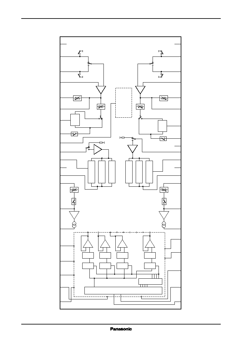
The AN7356NSC is an audio signal processing IC for
analog cassette deck. All the recording and playback pro-
cessing can be realized with one chip.
s
Features
∑
Control various adjustment circuit by serial data
∑
Playback system
∑ Built-in variable volume circuit (
±
6 dB) for playback
gain adjustment
∑ Built-in various equalizer switching circuit
∑ Built-in series mute circuit
∑
Recording system
∑ Built-in equalizer (freq. characteristics, gain) circuit of
middle and high frequencies
∑ Built-in volume circuit (
+
20 dB) for overall gain
adjustment
∑ With low frequency band boost pins
∑ Built-in drive circuit for current output
∑
With parallel data output
s
Applications
∑
Cassette deck (Hi-Fi)
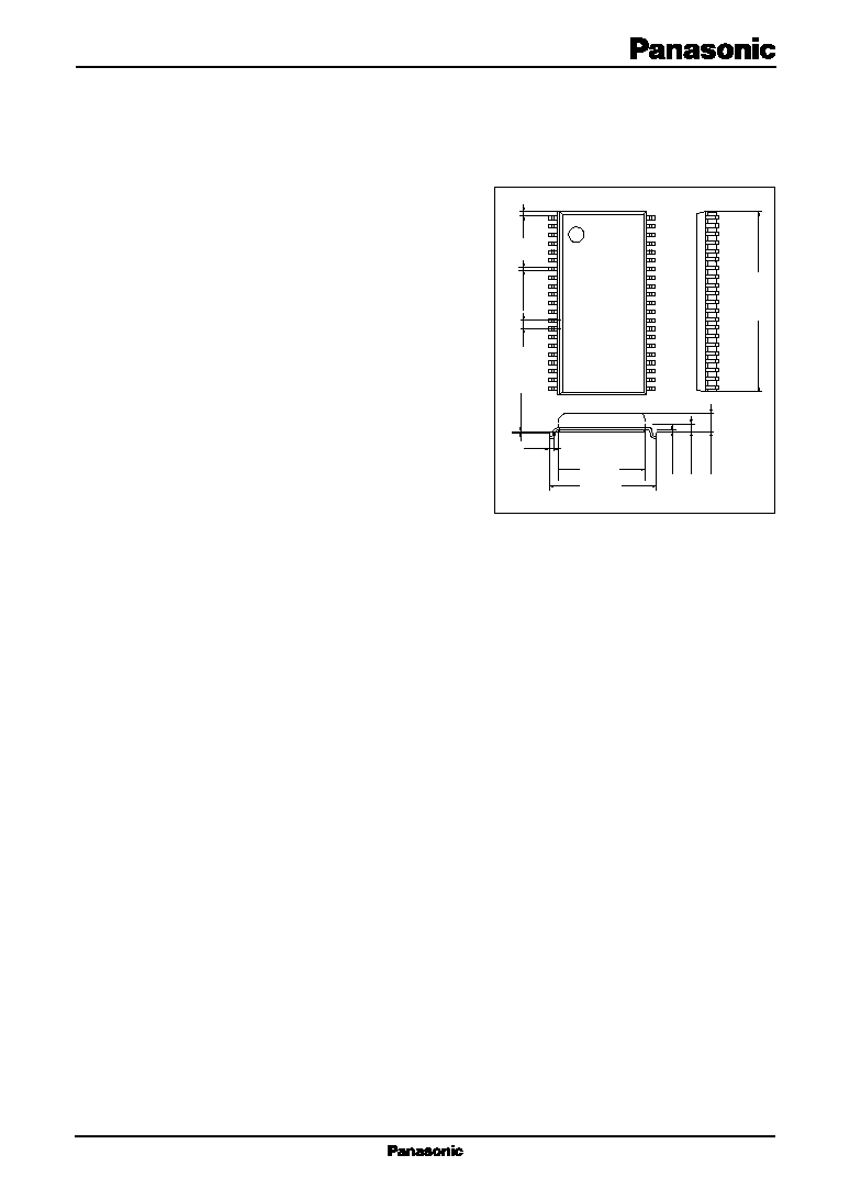
SSOP042-P-0450A
Unit: mm
0.3
1
21
42
22
21.25±0.3
11.5±0.3
0.35±0.1
2.0±0.2
1.0
0.9
0.1±0.1
9.5±0.3
0.45
0.15
ICs for Cassette/Cassette Deck Use
AN7356NSC
3
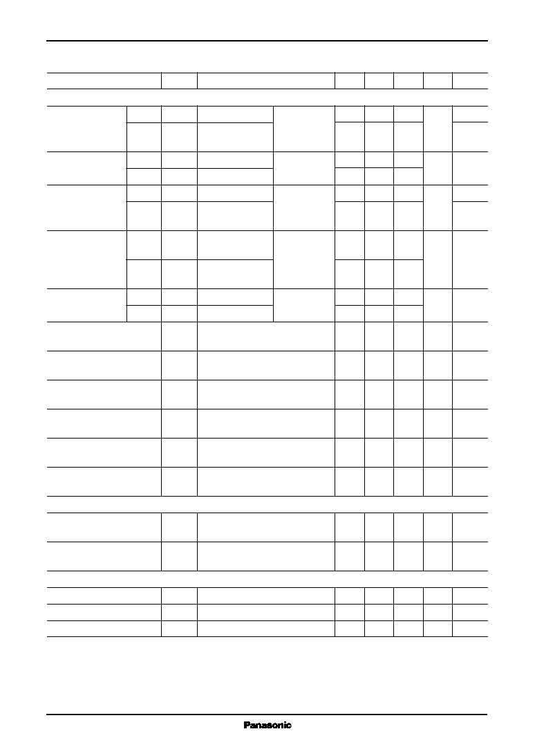
Parameter
Symbol
Rating
Unit
Supply voltage
V
CC
±
7.7
V
V
DD
+
7.7
Supply current
I
CC
mA
Power dissipation
*2
P
D
443
mW
Operating ambient temperature
*1
T
opr
-
25 to
+
75
∞
C
Storage temperature
*1
T
stg
-
55 to
+
150
∞
C
Pin No.
Description
1
Negative supply pin
2
Playback amp. TAPE1 input
3
Playback amp. TAPE2 input
4
Playback amp. negative feedback input
5
Playback amp. equalizer pin
6
Playback amp. negative feedback output
7
LPF pin
8
Playback amp. output
9
Positive supply pin
10
Recording amp. non-inverting input
11
Low frequency band boost pin
12
DAC output pin(Addr.: 02)
13
Recording equalizer amp. output
14
Recording volume amp. input
15
Recording amp. voltage output
16
Recording amp. current output
17
DAC output pin(Addr.: 0A)
18
DAC output pin (Addr.: 09)
19
FET drive current output
20
Negative supply pin
21
Erase current output
Pin No.
Description
22
Clock input
23
Serial data input
24
GND pin
25
Positive supply pin
26
Injector current pin
27
Recording amp. current output
28
Recording amp. voltage output
29
Recording volume amp. input
30
Recording equalizer amp. output
31
32
Low frequency band boost pin
33
Recording amp. non-inverting input
34
DAC calibration pin
35
Playback amp. output
36
LPF pin
37
Playback amp. negative feedback output
38
Playback amp. equalizer pin
39
Playback amp. negative feedback input
40
Playback amp. TAPE2 input
41
Playback amp. TAPE1 input
42
GND pin
s
Pin Descriptions
s
Absolute Maximum Ratings
Note) *1 : All items are at T
a
=
25
∞
C, except for the operating ambient temperature and storage temperature.
*2 : Power dissipation of the IC single unit at T
a
=
75
∞
C. Use the IC under the conditions of not exceeding the allowable power
dissipation curve.
s
Recommended Operating Range
Parameter
Symbol
Range
Unit
Supply voltage
V
CC
±
4.5 to
±
6.5 (typ.) to
±
7.2
V
V
DD
4.5 to 5.0 to
5.5
AN7356NSC
ICs for Cassette/Cassette Deck Use
4
Parameter
Symbol
Conditions
Min
Typ
Max
Unit
Note
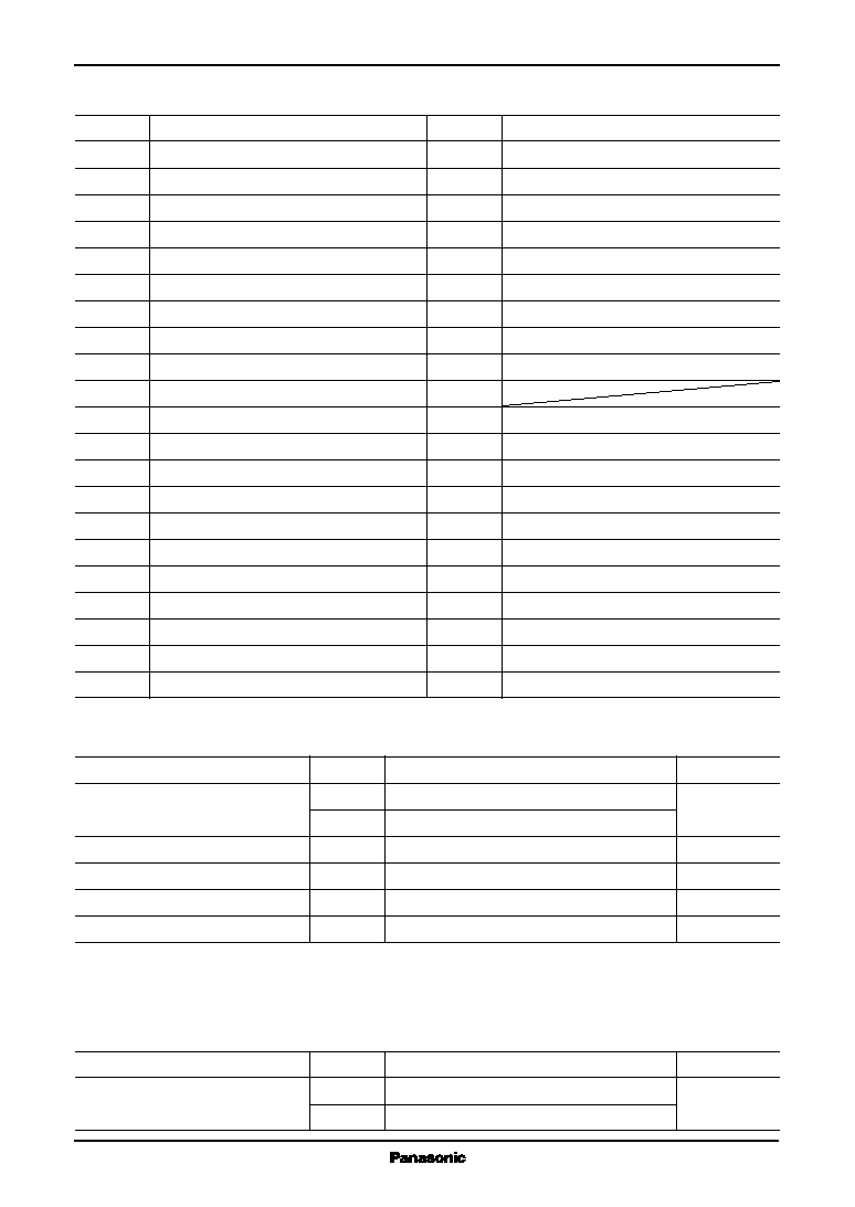
Playback system
V
IN
=
-
56 dBV, f
=
1 kHZ, 30 kHz LPF on
Reference output level (0 dB)
V
1
-
3.4
-
1.4
0.6
dBV
Data(1)
Reference output level (
+
6 dB)
G
H
Difference between 6 dB and 0 dB
5.0
6.0
7.0
dB
Data(2)
G
H
=
data (2)
-
data (1)
Reference output level (
-
6 dB)
G
L
Difference between
-
6 dB and 6 dB
10
11.8
13.5
dB
Data(3)
G
L
=
data (2)
-
data (3)
Level difference between
G
T12
Operation: The above reference output
0
1
dB
tapes
level (V
1
) difference between tapes
Total harmonic distortion (T1, 0 dB)
THD
1
V
IN
= -
64 dBV, 30 kHz LPF on
0.12
0.4
%
Total harmonic distortion (T2, 0 dB) THD
2
V
IN
= -
64 dBV, 30 kHz LPF on
0.12
0.4
%
Output noise voltage (T1, 0 dB)
V
NO1
IHF
-
A, R
g
=
2.2 k
-
69
-
56
dBV
Output noise voltage (T2, 0 dB)
V
NO2
IHF
-
A, R
g
=
2.2 k
-
69
-
56
dBV
Maximum output level (0 dB)
V
OMX
THD
=
3
%
2.0
3.6
dBV
Cross talk (ch. R
ch. L)
CT
1
R
g
(CH2)
=
220
60
dB
Cross talk (ch. L
ch. R)
CT
2
R
g
(CH1)
=
220
60
dB
Output offset voltage (0 dB)
V
OFF
R
g
=
220
-
450
+
130
mV
Mute attenuation (T2)
G
M0
DAC5
=
(08)
60
dB
Mute attenuation (T1)
G
M1
T2 mode
60
dB
Mute attenuation (T2)
G
M2
T1 mode
60
dB
Pulse noise voltage
V
P
R
g
=
2.2 k
0
9
mV
EQ-VR (120
µ
)
V
EQ120
f
=
10 kHz
-
7.3
-
5.3
-
3.3
dBV Data(17)
EQ-VR (70
µ
)
G
EQ70
f
=
10 kHz
-
5.0
-
4.0
-
3.0
dB
Data(18)
G
EQ70
=
data (18)
-
data (17)
EQ-VR (50
µ
)
G
EQ50
f
=
10 kHz
-
8.5
-
7.5
-
6.5
dB
Data(19)
G
EQ50
=
data (19)
-
data (17)
600 Hz LPF (50
µ
)
G
LPF
f
=
10 kHz
-
25
-
20
dB
Data(23)
G
LPF
=
data (23)
-
data (19)
T1/T2 switching shock noise
V
T12
Operation: The above output offset
-
55
0
55
mV
voltage (V
OFF
) difference between tapes
Recording system
Reference output (EQ output)
V
EQ
f
IN
=
400 Hz, V
IN
=
6 dBV
-
3
-
0.5
2.0
dBV
Middle and high
High
G
HH
V (400 Hz)
=
0 dB
f
IN
=
10 kHz
3.0
5.0
7.0
dB
Data (32H)
frequency gain
Low
G
HL
GHL
=
data
V
IN
=
-
12 dBV
10
13
15
Data (32L)
(32H)
-
data (32L)
High frequency
High
G
PH
V(400 Hz)
=
0 dB
f
IN
=
25 kHz
18
21
22
dB
Data (33H)
peak gain
Low
G
PL
GHL
=
data
V
IN
=
-
30 dBV
18
12
24
Data (33L)
(33H)
-
data (33L)
s
Electrical Characteristics at V
CC
=
±
6.5 V, T
a
=
25
∞
C