 | –≠–ª–µ–∫—Ç—Ä–æ–Ω–Ω—ã–π –∫–æ–º–ø–æ–Ω–µ–Ω—Ç: AN7560 | –°–∫–∞—á–∞—Ç—å:  PDF PDF  ZIP ZIP |
ICs for Audio Common Use
1
AN7555NZ
BTL output power IC for car audio
s
Overview
The AN7555NZ is an audio power IC developed as
the sound output of car audio (35 W
◊
4-channel). It has
realized the voltage gain of 40 dB based on the AN7560Z
(voltage gain: 34 dB). A capacitor and resistor to stop
oscillation are built in between the output pin and GND so
that a space saving of set is possible. Also, it incorpo-
rates a perfect muting circuit without shock noise, so that
a shock noise design under the set transient condition
can be made easily when used together with its standby
function. In addition, it incorporates various protection
circuits to protect the IC from destruction by GND-open
short circuit to ground, and power supply surge which are
the important subject of power IC protection. This IC
will largely contribute to a high reliability design of the
equipment.
s
Features
∑
A pattern layout in which input and output pattern do
not intersect each other on single-sided printed circuit
board is possible.
∑
Incorporating various protection circuits (temperature
protection, short circuit to V
CC
, V
CC
-open short circuit
to V
CC
, short circuit to GND, GND-open short circuit to
GND, overvoltage, power supply surge, and ASO, etc.)
∑
Built-in standby function (shock-noise free at STB-on/
off)
∑
Built-in muting function (shock-noise free at Mute-on/
off)
∑
External components reduction
∑
Provided with beep sound input pin
∑
Equipped with auxiliary sound input pin
∑
Voltage gain: 40 dB
(AN7560Z/AN7561Z: Voltage gain: 34 dB)
s
Applications
∑
Car stereo, miniature audio component, karaoke and
other audio equipment
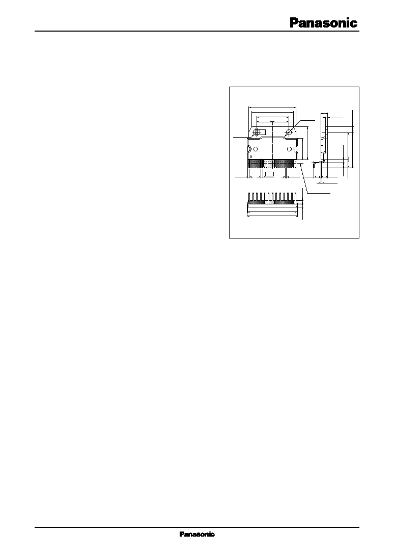
HZIP025-P-0980
Unit: mm
(10.50)
(10.50)
21.0±0.1
1.5±0.1
27.0±0.3
4.5±0.2
31.0±0.3
3.6±0.1
14.5±0.3
(1.95)
(2.15)
15.5±0.3
(3.30)
2.4±0.5
(5.70)
18.75±0.30
(24.45)
3.75±0.10
(1.26)
0.40
+0.2
≠0.1
+0.15
≠0.05
Seating plane
3.6±0.1
R1.8±0.1
0.6
(5.08)
(4.29)
1.27
1
25
33.0±0.3
33.36±0.30
2
AN7555NZ
ICs for Audio Common Use
s
Block Diagram
Pin No.
Description
1
Ch.4
+
output
2
GND (ch.4 output)
3
Ch.4
-
output
4
Supply voltage V
CC
5
Ch.3
+
output
6
GND (ch.3 output)
7
Ch.3
-
output
8
GND (ch.3 output)
9
Ch.2 + output
10
AUX input
11
Ch.2
-
output
12
Supply voltage Vcc
13
Ch.1
+
output
s
Pin Descriptions
Pin No.
Description
14
GND (ch.1 output)
15
Ch.1
-
output
16
Standby
17
Ch.1 input
18
Beep input
19
Ch.2 input
20
GND (input)
21
Ch.4 input
22
GND (printed circuit board)
23
Ch.3 input
24
Muting
25
Ripple filter
Ripple
filter
Beep
input
Protection
circuit
Attenuation
control
AUX
input
25
5
7
16
9
8
11
13
14
15
4
21
V
CC
12
19
V
CC
GND (sub)
22
23
18
Muting
Beep
GND (input)
24
GND (output)
GND (output)
Attenuator
Attenuator
GND (output)
GND (output)
6
10
17
AU
X
20
1
3
2
Note) It is not necessary to connect capacitor and resistor for stopping the oscillation at the output terminals.
Use them after check if necessary for noise countermeasure.
3
ICs for Audio Common Use
AN7555NZ
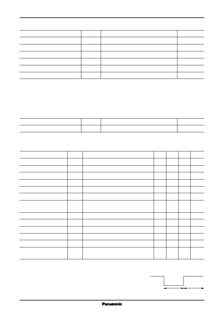
s
Electrical Characteristics at V
CC
=
13.2 V, f
=
1 kHz, T
a
=
25
∞
C
s
Absolute Maximum Ratings
Parameter
Symbol
Rating
Unit
Supply voltage
*2
V
CC
25
V
Peak supply voltage
*3
V
surge
65
V
Supply current
I
CC
12
A
Power dissipation
*4
P
D
59
W
Operating ambient temperature
*1
T
opr
-
30 to
+
85
∞
C
Storage temperature
*1
T
stg
-
55 to
+
150
∞
C
s
Recommended Operating Range
Parameter
Symbol
Range
Unit
Supply voltage
V
CC
8.0 to 18.0
V
Parameter
Symbol
Conditions
Min
Typ
Max
Unit
Quiescent current
I
CQ
R
g
=
10 k
, R
L
=
4
300
450
mA
Standby current
I
STB
R
g
=
10 k
, R
L
=
4
1
10
µ
A
Output noise voltage
*1
V
NO
R
g
=
10 k
, R
L
=
4
0.25
0.5
mV[rms]
Voltage gain
G
V
V
IN
=
20 mV, R
L
=
4
38
40
42
dB
Total harmonic distortion 1
THD1
V
IN
=
20 mV, R
L
=
4
0.05
0.2
%
Maximum output power
P
O
THD
=
10%, R
L
=
4
16
19.5
W
Ripple rejection
*1
RR
R
L
=
4
,
R
g
=
10 k
, V
R
=
1 V[rms],
55
65
dB
f
R
=
1 kHz
Channel balance
CB
V
IN
=
20 mV, R
L
=
4
0
1
dB
Cross-talk
CT
V
IN
=
20 mV, R
L
=
4
,
R
g
=
10 k
60
70
dB
Output offset voltage
V
OFF
R
g
=
10 k
, R
L
=
4
-
300
0
300
mV
Muting effect
*1
MT
V
IN
=
20 mV, R
L
=
4
70
80
dB
Input impedance
Z
I
V
IN
=
±
0.3 V
DC
24
30
36
k
Shock noise
*2
V
S
R
L
=
4
,
R
g
=
10 k
, V
MUTE
=
5 V,
-
100
0
100
mV[p-0]
V
STB
=
on/off, 50 Hz HPF
Note) *1 : T
a
=
25
∞
C except operating ambient temperature and storage temperature.
*2 : Without signal
*3 : Time
=
0.2 s
*4 : Power dissipation at T
a
=
85
∞
C
Note) *1 : Measurement using a bandwidth 15 Hz to 30 kHz (12 dB/OCT) filter.
*2 : Change over the standby terminal at the time shown in the right.
5 V
0 V
Standby terminal voltage
500 ms
500 ms
4
AN7555NZ
ICs for Audio Common Use
s
Usage Notes
1. Always attach an outside heat sink to use the AN7555NZ. In addition, the outside heat sink must be fastened onto
a chassis for use.
2. Connect the radiation fin to the GND potential.
3. Prevent short circuit to V
CC
and short circuit to GND, and load short-circuit although the protection circuits for short
circuit to V
CC
and ASO are built-in.
4. The thermal protection circuit gets actuated when T
j
=
approx. 150
∞
C, but it is automatically reset when the chip
temperature drops below the above set level.
5. The overvoltage protection circuit starts the protection operation at V
CC
=
approx. 20 V.
6. Take into consideration the heat radiation design particularly when V
CC
is set high.
7. When the beep sound function is not used, connect to GND the beep sound input pin.
8. Don't down below
-
0.3 V for the beep sound input pin.
9. When the AUX function is not used, open the AUX input pin.
10. Connect to signal GND of pre-stage amplifier only for the signal source ground.
∑
There are the possibility of breakdown for the following conditions.
1. Reverse connection of the power supply pin and the GND pin.
2. Connection of the power supply between output pins at open condition of the power supply pin and the GND pin.
3. Short circuit to GND of output pin when the GND pin is open.
4. Short circuit to GND of above the three output pins at the same time with a shorting resistor which does not
operate the protection circuit.
5. Short circuit to GND of above the plus and minus output pins at the same time with a shorting resistor which does
not operate the protection circuit.
6. Short circuit to ground with shorting the RF pin and the output pin.
s
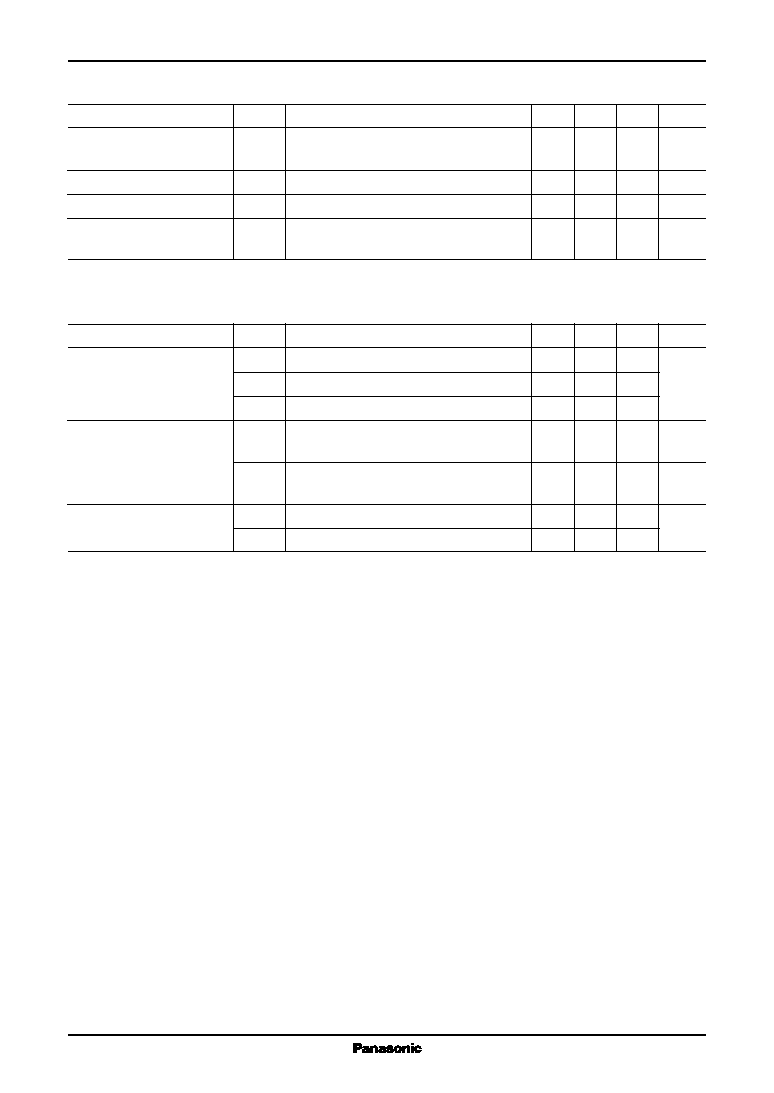
Electrical Characteristics at V
CC
=
13.2 V, f
=
1 kHz, T
a
=
25
∞
C (continued)
Parameter
Symbol
Conditions
Min
Typ
Max
Unit
Total harmonic distortion 2
THD2
V
IN
=
10 mV, f
IN
=
20 kHz, R
g
=
10
,
0.1
0.5
%
R
L
=
Mute-on threshold voltage
MT
ON
V
IN
=
20 mV, R
L
=
4
4
V
Mute-off threshold voltage
MT
OFF
V
IN
=
20 mV, R
L
=
4
0.8
V
Cutoff frequency
f
C
V
IN
=
20 mV, R
L
=
4
,
20
40
kHz
G
V
=
-
1 dB (0 dB: 1 kHz)
∑
Design reference data
Note) The characteristic values below are theoretical values for designing and not guaranteed.
Parameter
Symbol
Conditions
Min
Typ
Max
Unit
Maximum output power
P
Omax
Max. power, R
L
=
4
28
W
P
O2
V
CC
=
14.4 V, THD
=
10%, R
L
=
4
21
P
Omax2
V
CC
=
14.4 V, max. power, R
L
=
4
34
Power band width
f
PL
V
CC
=
14.4 V, THD
=
1%, R
L
=
4
,
10
Hz
PoL
= -
3 dB (1 kHz: 0 dB)
f
PH
V
CC
=
14.4 V, THD
=
1%, R
L
=
4
,
18
kHz
PoH
= -
3 dB (1 kHz: 0 dB)
STB threshold voltage
V
STB1
R
g
=
10 k
, R
L
=
4
, STB
ACT
2.2
V
V
STB2
R
g
=
10 k
, R
L
=
4
, ACT
STB
1.5
5
ICs for Audio Common Use
AN7555NZ
s
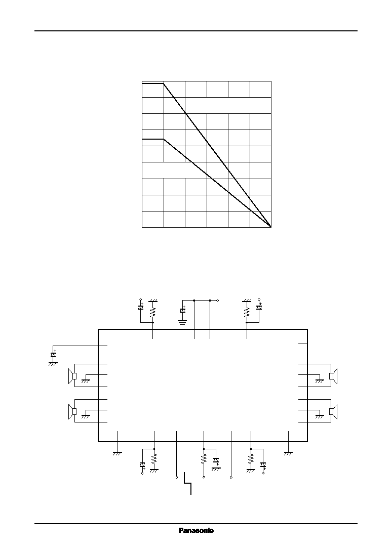
Technical Information
∑
P
D
T
a
curves of HZIP025-P-0980
P
D
T
a
1.800
1.770
0.000
0
25
150
0.200
Ambient temperature T
a
(∞
C)
Po
wer dissipation P
D
(W)
0.400
0.600
0.800
1.000
1.075
1.200
1.400
1.600
50
75
100
125
Mounted on standard board
(grass epoxy : 50 mm
◊
50 mm
◊
t0.08 mm)
R
th (j
-
a)
=
70.6
∞
C/W
Independent IC
without heat shink
R
th( j
-
a)
=
116.2
∞
C/W
s
Application Circuit Example
2
1
3
16
13
4
12
21
19
22 k
Muting
24
23
17
10
22
15
25
14
20
4
6
5
7
4
4
33
µ
F
V
CC
4
9
11
8
10 k
1
µ
F
10 k
1
µ
F
2 200
µ
F
1
µ
F
10 k
1
µ
F
AU
X
18
Beep
10 k
1
µ
F
5 V
0 V