 | –≠–ª–µ–∫—Ç—Ä–æ–Ω–Ω—ã–π –∫–æ–º–ø–æ–Ω–µ–Ω—Ç: AN7800 | –°–∫–∞—á–∞—Ç—å:  PDF PDF  ZIP ZIP |
s Overview
The AN7800 series and the AN7800F series are 3-pin
fixed positive output voltage regulators. Stabilized fixed
output voltage is obtained from unstable DC input volt-
age without using external components. 11 types of fixed
output voltage are available, 5V, 6V, 7V, 8V, 9V, 10V,
12V, 15V, 18V, 20V and 24V. They can be used widely in
power circuits with current capacity up to 1A.
s Features
∑ No external components
∑ Output voltage:5V, 6V, 7V, 8V, 9V, 10V,
12V, 15V, 18V, 20V, 24V
∑ Internal short-circuit current limiting
∑ Internal thermal overload protection
∑ Output transistor safe area compensation
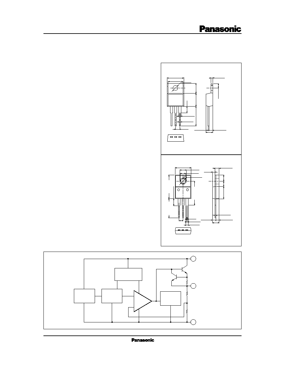
AN7800/AN7800F Series
3-pin Positive Output Voltage Regulator (1A Type)
Unit:mm
AN7800 Series
10.4
±
0.5
1.4
±
0.1
2.9
±
0.1
6.7
±
0.25
8.7
±
0.3
13.6
±
0.25
1.4
±
0.25
4.5
¯3.7
10.5
±
0.5
JEDEC:TO-220AB (HSIP003-P-0000)
2.54
0.45
1:Input
2:Common
3:Output
2.5
±
0.25
+ 0.1
≠ 0.05
1
2
3
4.5
±
0.3
0.8
±
0.2
Unit:mm
AN7800F Series
(4.3)
10.5
±
0.3
2.77
±
0.3
(1.73)
¯5.3
16.7
±
0.3
17.0
±
0.25
4.2
±
0.25
3.8
±
0.25
8.7
±
0.3
13.6
±
0.25
4.5
±
0.25
(0.4)
0.4
+ 0.1
≠ 0.05
0.8
±
0.2
2.5
±
0.25
2.0
±
0.25
4.5
±
0.3
2.54
1 2 3
1.4
±
0.2
3.1
±
0.1
TO-220 Full Pack Package (HSIP003-P-0000A)
1:Input
2:Common
3:Output
s Block Diagram
1
3
2
Input
Pass Tr
Output
Common
Starter
Voltage
Reference
Current
Source
ErrorAmp.
+
≠
Thermal
Protection
Q
1
R
SC
R
2
R
1
Current
Limiter
V
I
P
D
T
opr
T
stg
V
V
W
∞C
∞C
s Absolute Maximum Ratings (Ta=25∞C)
35 *
1
40 *
2
15 *
3
10.25 *
3
≠30 to+80
≠55 to+150
AN7800 Series
AN7800F Series
Input voltage
Power dissipation
Operating ambient temperature
Storage temperature
*1 AN7805/F, AN7806/F, AN7807/F, AN7808/F, AN7809/F, AN7810/F, AN7812/F, AN7815/F, AN7818/F
*2 AN7820/F, AN7824/F
*3 Follow the derating curve. When T
j
exceeds 150∞C, the internal circuit cuts off output.
Parameter
Symbol
Rating
Unit
V
O
5.2
V
5
T
j
=25∞C
V
O
V
V
I
=8 to 20V, I
O
=5mA to 1A,
T
j
=0 to 125∞C, P
D
*
REG
IN
100
mV
3
V
I
=7.5 to 25V, T
j
=25∞C
mV
REG
L
mV
15
I
O
=5mA to 1.5A, T
j
=25∞C
mV
I
O
=250 to 750mA, T
j
=25∞C
V
I
=8 to 12V, T
j
=25∞C
mA
3.9
T
j
=25∞C
1
I
bias
mA
V
I
=7.5 to 25V, T
j
=25∞C
I
bias (IN)
mA
I
bias (L)
µ
V
40
I
O
=5mA to 1A, T
j
=25∞C
V
no
dB
f=10Hz to 100kHz
1.3
0.5
50
5.25
100
50
8
62
4.8
4.75
RR
V
I
=8 to 18V, I
O
=100mA, f=120Hz
V
2
I
O
=1A, T
j
=25∞C
V
DIF (min.)
m
17
Z
O
mA
700
f=1kHz
I
O (Short)
A
2
V
I
=25V, T
j
=25∞C
5
I
O (Peak)
T
j
=25∞C
mV/∞C
≠ 0.3
V
O
/Ta
I
O
=5mA, T
j
=0 to 125∞C
Output voltage
Output voltage tolerance
Line regulation
Load regulation
Note 1) The specified condition T
j
=25∞C means that the test should be carried out with the test time so short (within 10ms) that the
drift in characteristic value due to the rise in chip junction temperature can be ignored.
Note 2) When not specified, V
I
=10V, I
O
=500mA, C
I
=0.33
µ
F and C
O
=0.1
µ
F.
* AN7800 Series:15W, AN7800F Series:10.25W
Bias current
Input bias current change
Load bias current change
Output noise voltage
Ripple rejection ratio
Minimum input/output voltage difference
Output short circuit current
Output impedance
Peak output current
Output voltage temperature coefficient
s Electrical Characteristics (Ta=25∞C)
∑
AN7805/7805F (5V Type)
Parameter
Symbol
Condition
min
typ
max
Unit
=
<
V
O
6.25
V
6
V
O
V
V
I
=9 to 21V, I
O
=5mA to 1A,
T
j
=0 to 125∞C, P
D
*
REG
IN
120
mV
5
V
I
=8.5 to 25V, T
j
=25∞C
mV
REG
L
mV
14
I
O
=5mA to 1.5A, T
j
=25∞C
mV
I
O
=250 to 750mA, T
j
=25∞C
V
I
=9 to 13V, T
j
=25∞C
mA
3.9
T
j
=25∞C
1.5
I
bias
mA
V
I
=8.5 to 25V, T
j
=25∞C
mA
40
I
O
=5mA to 1A, T
j
=25∞C
V
no
dB
f=10Hz to 100kHz
1.3
0.5
60
6.3
120
60
8
59
5.75
5.7
RR
V
I
=9 to 19V, I
O
=100mA, f=120Hz
V
2
I
O
=1A, T
j
=25∞C
17
Z
O
mA
700
f=1kHz
A
2
V
I
=25V, T
j
=25∞C
4
T
j
=25∞C
≠ 0.4
I
O
=5mA, T
j
=0 to 125∞C
Output voltage
Output voltage tolerance
Line regulation
Load regulation
Bias current
Input bias current change
Load bias current change
Output noise voltage
Ripple rejection ratio
Minimum input/output voltage difference
Output short circuit current
Output impedance
Peak output current
Output voltage temperature coefficient
Parameter
Symbol
Condition
min
typ
max
Unit
T
j
=25∞C
I
bias (IN)
I
bias (L)
µ
V
V
DIF (min.)
m
I
O (Short)
I
O (Peak)
mV/∞C
V
O
/Ta
Note 1) The specified condition T
j
=25∞C means that the test should be carried out with the test time so short (within 10ms) that the
drift in characteristic value due to the rise in chip junction temperature can be ignored.
Note 2) When not specified, V
I
=11V, I
O
=500mA, C
I
=0.33
µ
F and C
O
=0.1
µ
F.
* AN7800 Series:15W, AN7800F Series:10.25W
s Electrical Characteristics (Ta=25∞C)
∑
AN7806/7806F (6V Type)
=
<
V
O
7.3
V
7
T
j
=25∞C
V
O
V
V
I
=10 to 22V, I
O
=5mA to 1A,
T
j
=0 to 125∞C, P
D
*
REG
IN
140
mV
5
V
I
=9.5 to 25V, T
j
=25∞C
mV
REG
L
mV
14
I
O
=5mA to 1.5A, T
j
=25∞C
mV
I
O
=250 to 750mA, T
j
=25∞C
V
I
=10 to 15V, T
j
=25∞C
mA
3.9
T
j
=25∞C
1.5
I
bias
mA
V
I
=9.5 to 25V, T
j
=25∞C
mA
46
I
O
=5mA to 1A, T
j
=25∞C
V
no
dB
f=10Hz to 100kHz
1
0.5
70
7.4
140
70
8
57
6.7
6.6
RR
V
I
=10 to 20V, I
O
=100mA, f=120Hz
V
2
I
O
=1A, T
j
=25∞C
16
Z
O
mA
700
f=1kHz
A
2
V
I
=25V, T
j
=25∞C
4
T
j
=25∞C
≠ 0.5
I
O
=5mA, T
j
=0 to 125∞C
Output voltage
Output voltage tolerance
Line regulation
Load regulation
Bias current
Input bias current change
Load bias current change
Output noise voltage
Ripple rejection ratio
Minimum input/output voltage difference
Output short circuit current
Output impedance
Peak output current
Output voltage temperature coefficient
Parameter
Symbol
Condition
min
typ
max
Unit
I
bias (IN)
I
bias (L)
µ
V
V
DIF (min.)
m
I
O (Short)
I
O (Peak)
mV/∞C
V
O
/Ta
Note 1) The specified condition T
j
=25∞C means that the test should be carried out with the test time so short (within 10ms) that the
drift in characteristic value due to the rise in chip junction temperature can be ignored.
Note 2) When not specified, V
I
=12V, I
O
=500mA, C
I
=0.33
µ
F and C
O
=0.1
µ
F.
* AN7800 Series:15W, AN7800F Series:10.25W
∑
AN7807/7807F (7V Type)
=
<

V
O
8.3
V
8
T
j
=25∞C
V
O
V
V
I
=11 to 23V, I
O
=5mA to 1A,
T
j
=0 to 125∞C, P
D
*
REG
IN
160
mV
6
V
I
=10.5 to 25V, T
j
=25∞C
mV
REG
L
mV
12
I
O
=5mA to 1.5A, T
j
=25∞C
mV
I
O
=250 to 750mA, T
j
=25∞C
V
I
=11 to 17V, T
j
=25∞C
mA
3.9
T
j
=25∞C
2
I
bias
mA
V
I
=10.5 to 25V, T
j
=25∞C
mA
52
I
O
=5mA to 1A, T
j
=25∞C
V
no
dB
f=10Hz to 100kHz
1
0.5
80
8.4
160
80
8
56
7.7
7.6
RR
V
I
=11.5 to 21.5V, I
O
=100mA, f=120Hz
V
2
I
O
=1A, T
j
=25∞C
16
Z
O
mA
700
f=1kHz
A
2
V
I
=25V, T
j
=25∞C
4
T
j
=25∞C
≠ 0.5
I
O
=5mA, T
j
=0 to 125∞C
Output voltage
Output voltage tolerance
Line regulation
Load regulation
Bias current
Input bias current change
Load bias current change
Output noise voltage
Ripple rejection ratio
Minimum input/output voltage difference
Output short circuit current
Output impedance
Peak output current
Output voltage temperature coefficient
Parameter
Symbol
Condition
min
typ
max
Unit
I
bias (IN)
I
bias (L)
µ
V
V
DIF (min.)
m
I
O (Short)
I
O (Peak)
mV/∞C
V
O
/Ta
Note 1) The specified condition T
j
=25∞C means that the test should be carried out with the test time so short (within 10ms) that the
drift in characteristic value due to the rise in chip junction temperature can be ignored.
Note 2) When not specified, V
I
=14V, I
O
=500mA, C
I
=0.33
µ
F and C
O
=0.1
µ
F.
* AN7800 Series:15W, AN7800F Series:10.25W
s Electrical Characteristics (Ta=25∞C)
∑
AN7808/7808F (8V Type)
=
<
V
O
9.35
V
9
T
j
=25∞C
V
O
V
V
I
=12 to 24V, I
O
=5mA to 1A,
T
j
=0 to 125∞C, P
D
*
REG
IN
180
mV
7
V
I
=11.5 to 26V, T
j
=25∞C
mV
REG
L
mV
12
I
O
=5mA to 1.5A, T
j
=25∞C
mV
I
O
=250 to 750mA, T
j
=25∞C
V
I
=12 to 18V, T
j
=25∞C
mA
3.9
T
j
=25∞C
2
I
bias
mA
V
I
=11.5 to 26V, T
j
=25∞C
mA
57
I
O
=5mA to 1A, T
j
=25∞C
V
no
dB
f=10Hz to 100kHz
1
0.5
90
9.45
180
90
8
56
8.65
8.55
RR
V
I
=12 to 22V, I
O
=100mA, f=120Hz
V
2
I
O
=1A, T
j
=25∞C
16
Z
O
mA
700
f=1kHz
A
2
V
I
=26V, T
j
=25∞C
4
T
j
=25∞C
≠ 0.5
I
O
=5mA, T
j
=0 to 125∞C
Output voltage
Output voltage tolerance
Line regulation
Load regulation
Bias current
Input bias current change
Load bias current change
Output noise voltage
Ripple rejection ratio
Minimum input/output voltage difference
Output short circuit current
Output impedance
Peak output current
Output voltage temperature coefficient
Parameter
Symbol
Condition
min
typ
max
Unit
I
bias (IN)
I
bias (L)
µ
V
V
DIF (min.)
m
I
O (Short)
I
O (Peak)
mV/∞C
V
O
/Ta
Note 1) The specified condition T
j
=25∞C means that the test should be carried out with the test time so short (within 10ms) that the
drift in characteristic value due to the rise in chip junction temperature can be ignored.
Note 2) When not specified, V
I
=15V, I
O
=500mA, C
I
=0.33
µ
F and C
O
=0.1
µ
F.
* AN7800 Series:15W, AN7800F Series:10.25W
∑
AN7809/7809F (9V Type)
=
<
V
O
10.4
V
10
T
j
=25∞C
V
O
V
V
I
=13 to 25V, I
O
=5mA to 1A,
T
j
=0 to 125∞C, P
D
*
REG
IN
200
mV
8
V
I
=12.5 to 27V, T
j
=25∞C
mV
REG
L
mV
12
I
O
=5mA to 1.5A, T
j
=25∞C
mV
I
O
=250 to 750mA, T
j
=25∞C
V
I
=13 to 19V, T
j
=25∞C
mA
3.9
T
j
=25∞C
2.5
I
bias
mA
V
I
=12.5 to 27V, T
j
=25∞C
mA
63
I
O
=5mA to 1A, T
j
=25∞C
V
no
dB
f=10Hz to 100kHz
1
0.5
100
10.5
200
100
8
56
9.6
9.5
RR
V
I
=13 to 23V, I
O
=100mA, f=120Hz
V
2
I
O
=1A, T
j
=25∞C
16
Z
O
mA
700
f=1kHz
A
2
V
I
=27V, T
j
=25∞C
4
T
j
=25∞C
≠ 0.6
I
O
=5mA, T
j
=0 to 125∞C
Output voltage
Output voltage tolerance
Line regulation
Load regulation
Bias current
Input bias current change
Load bias current change
Output noise voltage
Ripple rejection ratio
Minimum input/output voltage difference
Output short circuit current
Output impedance
Peak output current
Output voltage temperature coefficient
Parameter
Symbol
Condition
min
typ
max
Unit
I
bias (IN)
I
bias (L)
V
DIF (min.)
I
O (Short)
I
O (Peak)
mV/∞C
V
O
/Ta
Note 1) The specified condition T
j
=25∞C means that the test should be carried out with the test time so short (within 10ms) that the
drift in characteristic value due to the rise in chip junction temperature can be ignored.
Note 2) When not specified, V
I
=16V, I
O
=500mA, C
I
=0.33
µ
F and C
O
=0.1
µ
F.
* AN7800 Series:15W, AN7800F Series:10.25W
s Electrical Characteristics (Ta=25∞C)
∑
AN7810/7810F (10V Type)
=
<
µ
V
m
V
O
12.5
V
12
T
j
=25∞C
V
O
V
V
I
=15 to 27V, I
O
=5mA to 1A,
T
j
=0 to 125∞C, P
D
*
REG
IN
240
mV
10
V
I
=14.5 to 30V, T
j
=25∞C
mV
REG
L
mV
12
I
O
=5mA to 1.5A, T
j
=25∞C
mV
I
O
=250 to 750mA, T
j
=25∞C
V
I
=16 to 22V, T
j
=25∞C
mA
4
T
j
=25∞C
3
I
bias
mA
V
I
=14.5 to 30V, T
j
=25∞C
mA
75
I
O
=5mA to 1A, T
j
=25∞C
V
no
dB
f=10Hz to 100kHz
1
0.5
120
12.6
240
120
8
55
11.5
11.4
RR
V
I
=15 to 25V, I
O
=100mA, f=120Hz
V
2
I
O
=1A, T
j
=25∞C
18
Z
O
mA
700
f=1kHz
A
2
V
I
=30V, T
j
=25∞C
4
T
j
=25∞C
≠ 0.8
I
O
=5mA, T
j
=0 to 125∞C
Output voltage
Output voltage tolerance
Line regulation
Load regulation
Bias current
Input bias current change
Load bias current change
Output noise voltage
Ripple rejection ratio
Minimum input/output voltage difference
Output short circuit current
Output impedance
Peak output current
Output voltage temperature coefficient
Parameter
Symbol
Condition
min
typ
max
Unit
I
bias (IN)
I
bias (L)
µ
V
V
DIF (min.)
m
I
O (Short)
I
O (Peak)
mV/∞C
V
O
/Ta
Note 1) The specified condition T
j
=25∞C means that the test should be carried out with the test time so short (within 10ms) that the
drift in characteristic value due to the rise in chip junction temperature can be ignored.
Note 2) When not specified, V
I
=19V, I
O
=500mA, C
I
=0.33
µ
F and C
O
=0.1
µ
F.
* AN7800 Series:15W, AN7800F Series:10.25W
∑
AN7812/7812F (12V Type)
=
<
V
O
15.6
V
15
T
j
=25∞C
V
O
V
V
I
=18 to 30V, I
O
=5mA to 1A,
T
j
=0 to 125∞C, P
D
*
REG
IN
300
mV
11
V
I
=17.5 to 30V, T
j
=25∞C
mV
REG
L
mV
12
I
O
=5mA to 1.5A, T
j
=25∞C
mV
I
O
=250 to 750mA, T
j
=25∞C
V
I
=20 to 26V, T
j
=25∞C
mA
4
T
j
=25∞C
3
I
bias
mA
V
I
=17.5 to 30V, T
j
=25∞C
mA
90
I
O
=5mA to 1A, T
j
=25∞C
V
no
dB
f=10Hz to 100kHz
1
0.5
150
15.75
300
150
8
54
14.4
14.25
RR
V
I
=18.5 to 28.5V, f=120Hz
V
2
I
O
=1A, T
j
=25∞C
19
Z
O
mA
700
f=1kHz
A
2
V
I
=30V, T
j
=25∞C
4
T
j
=25∞C
≠1
I
O
=5mA, T
j
=0 to 125∞C
Output voltage
Output voltage tolerance
Line regulation
Load regulation
Bias current
Input bias current change
Load bias current change
Output noise voltage
Ripple rejection ratio
Minimum input/output voltage difference
Output short circuit current
Output impedance
Peak output current
Output voltage temperature coefficient
Parameter
Symbol
Condition
min
typ
max
Unit
I
bias (IN)
I
bias (L)
µ
V
V
DIF (min.)
m
I
O (Short)
I
O (Peak)
mV/∞C
V
O
/Ta
Note 1) The specified condition T
j
=25∞C means that the test should be carried out with the test time so short (within 10ms) that the
drift in characteristic value due to the rise in chip junction temperature can be ignored.
Note 2) When not specified, V
I
=23V, I
O
=500mA, C
I
=0.33
µ
F and C
O
=0.1
µ
F.
* AN7800 Series:15W, AN7800F Series:10.25W
s Electrical Characteristics (Ta=25∞C)
∑
AN7815/7815F (15V Type)
=
<
V
O
18.7
V
18
T
j
=25∞C
V
O
V
V
I
=21 to 33V, I
O
=5mA to 1A,
T
j
=0 to 125∞C, P
D
*
REG
IN
360
mV
14
V
I
=21 to 33V, T
j
=25∞C
mV
REG
L
mV
12
I
O
=5mA to 1.5A, T
j
=25∞C
mV
I
O
=250 to 750mA, T
j
=25∞C
V
I
=24 to 30V, T
j
=25∞C
mA
4.1
T
j
=25∞C
4
I
bias
mA
V
I
=21 to 33V, T
j
=25∞C
mA
110
I
O
=5mA to 1A, T
j
=25∞C
V
no
dB
f=10Hz to 100kHz
1
0.5
180
18.9
360
180
8
53
17.3
17.1
RR
V
I
=22 to 32V, I
O
=100mA, f=120Hz
V
2
I
O
=1A, T
j
=25∞C
16
Z
O
mA
700
f=1kHz
A
2
V
I
=35V, T
j
=25∞C
4
T
j
=25∞C
≠1.1
I
O
=5mA, T
j
=0 to 125∞C
Output voltage
Output voltage tolerance
Line regulation
Load regulation
Bias current
Input bias current change
Load bias current change
Output noise voltage
Ripple rejection ratio
Minimum input/output voltage difference
Output short circuit current
Output impedance
Peak output current
Output voltage temperature coefficient
Parameter
Symbol
Condition
min
typ
max
Unit
I
bias (IN)
I
bias (L)
µ
V
V
DIF (min.)
m
I
O (Short)
I
O (Peak)
mV/∞C
V
O
/Ta
Note 1) The specified condition T
j
=25∞C means that the test should be carried out with the test time so short (within 10ms) that the
drift in characteristic value due to the rise in chip junction temperature can be ignored.
Note 2) When not specified, V
I
=27V, I
O
=500mA, C
I
=0.33
µ
F and C
O
=0.1
µ
F.
* AN7800 Series:15W, AN7800F Series:10.25W
∑
AN7818/7818F (18V Type)
=
<
V
O
20.8
V
20
T
j
=25∞C
V
O
V
V
I
=24 to 35V, I
O
=5mA to 1A,
T
j
=0 to 125∞C, P
D
*
REG
IN
400
mV
15
V
I
=23 to 35V, T
j
=25∞C
mV
REG
L
mV
12
I
O
=5mA to 1.5A, T
j
=25∞C
mV
I
O
=250 to 750mA, T
j
=25∞C
V
I
=26 to 32V, T
j
=25∞C
mA
4.1
T
j
=25∞C
5
I
bias
mA
V
I
=23 to 35V, T
j
=25∞C
mA
110
I
O
=5mA to 1A, T
j
=25∞C
V
no
dB
f=10Hz to 100kHz
1
0.5
200
21
400
200
8
53
19.2
19
RR
V
I
=24 to 34V, I
O
=100mA, f=120Hz
V
2
I
O
=1A, T
j
=25∞C
22
Z
O
mA
700
f=1kHz
A
2
V
I
=35V, T
j
=25∞C
4
T
j
=25∞C
≠1.2
I
O
=5mA, T
j
=0 to 125∞C
Output voltage
Output voltage Tolerance
Line regulation
Load regulation
Bias current
Input bias current change
Load bias current change
Output noise voltage
Ripple rejection ratio
Minimum input/output voltage difference
Output short circuit current
Output impedance
Peak output current
Output voltage temperature coefficient
Parameter
Symbol
Condition
min
typ
max
Unit
I
bias (IN)
I
bias (L)
V
DIF (min.)
I
O (Short)
I
O (Peak)
mV/∞C
V
O
/Ta
Note 1) The specified condition T
j
=25∞C means that the test should be carried out with the test time so short (within 10ms) that the
drift in characteristic value due to the rise in chip junction temperature can be ignored.
Note 2) When not specified, V
I
=29V, I
O
=500mA, C
I
=0.33
µ
F and C
O
=0.1
µ
F.
* AN7800 Series:15W, AN7800F Series:10.25W
s Electrical Characteristics (Ta=25∞C)
∑
AN7820/7820F (20V Type)
=
<
µ
V
m
V
O
25
V
24
T
j
=25∞C
V
O
V
V
I
=28 to 38V, I
O
=5mA to 1A,
T
j
=0 to 125∞C, P
D
*
REG
IN
480
mV
18
V
I
=27 to 38V, T
j
=25∞C
mV
REG
L
mV
12
I
O
=5mA to 1.5A, T
j
=25∞C
mV
I
O
=250 to 750mA, T
j
=25∞C
V
I
=30 to 36V, T
j
=25∞C
mA
4.1
T
j
=25∞C
6
I
bias
mA
V
I
=27 to 38V, T
j
=25∞C
mA
170
I
O
=5mA to 1A, T
j
=25∞C
V
no
dB
f=10Hz to 100kHz
1
0.5
240
25.2
480
240
8
50
23
22.8
RR
V
I
=28 to 38V, I
O
=100mA, f=120Hz
V
2
I
O
=1A, T
j
=25∞C
28
Z
O
mA
700
f=1kHz
A
2
V
I
=38V, T
j
=25∞C
4
T
j
=25∞C
≠1.4
I
O
=5mA, T
j
=0 to 125∞C
Output voltage
Output voltage tolerance
Line regulation
Load regulation
Bias current
Input bias current change
Load bias current change
Output noise voltage
Ripple rejection ratio
Minimum input/output voltage difference
Output short circuit current
Output impedance
Peak output current
Output voltage temperature coefficient
∑
AN7824/7824F (24V Type)
Parameter
Symbol
Condition
min
typ
max
Unit
I
bias (IN)
I
bias (L)
V
DIF (min.)
I
O (Short)
I
O (Peak)
mV/∞C
V
O
/Ta
Note 1) The specified condition T
j
=25∞C means that the test should be carried out with the test time so short (within 10ms) that the
drift in characteristic value due to the rise in chip junction temperature can be ignored.
Note 2) When not specified, V
I
=33V, I
O
=500mA, C
I
=0.33
µ
F and C
O
=0.1
µ
F.
* AN7800 Series:15W, AN7800F Series:10.25W
=
<
µ
V
m
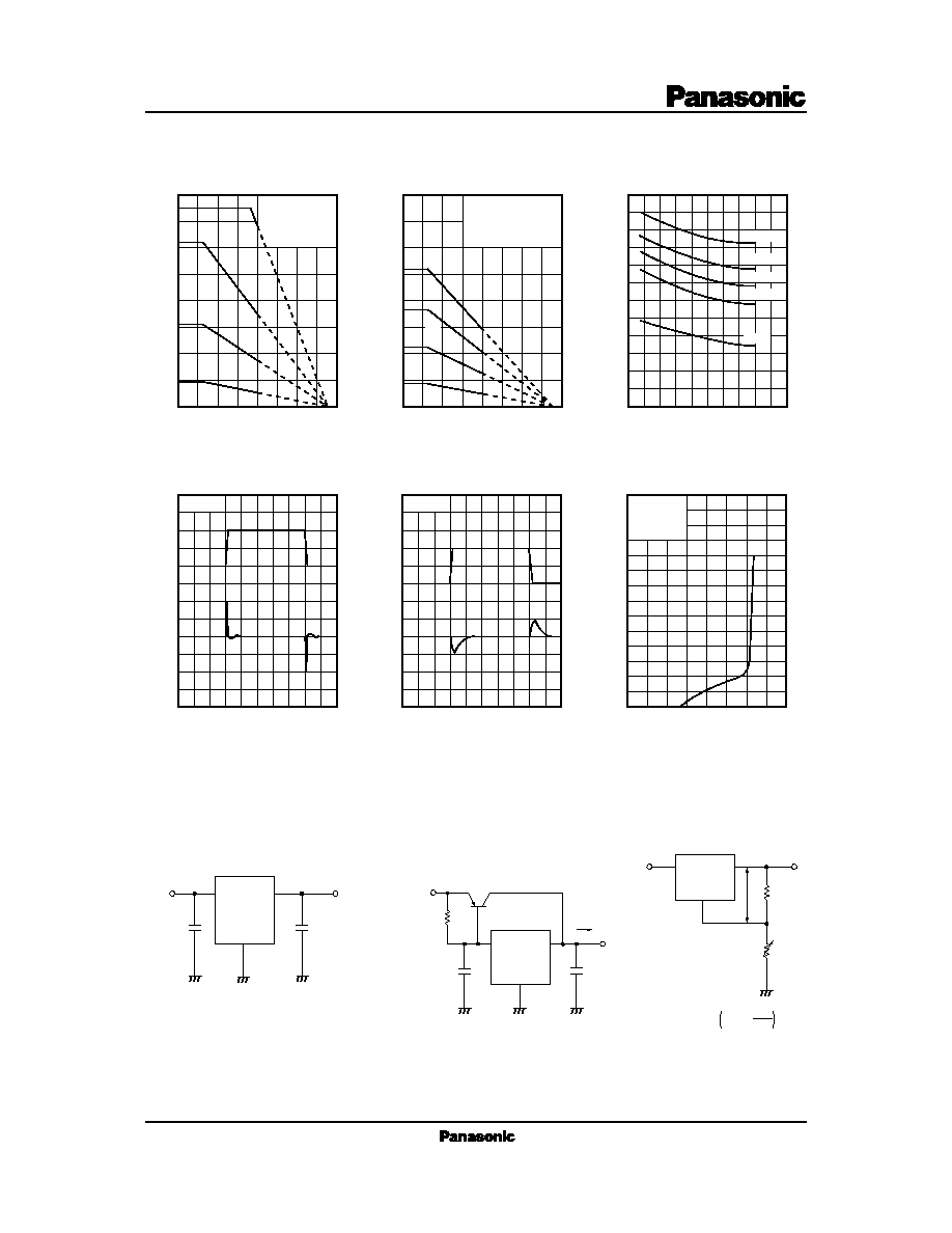
s Characteristic Curve
s Application Circuit
V
O
V
O
V
O
0.33
µ
F
0.1
µ
F
V
I
V
I
I
O
I
bias
V
O
= V
O
+ I
bias
+ R
1
R
2
V
O
3
Q
1
AN7800
AN7800F
AN7800
AN7800F
1) Current Boost Circuit
2) Adjustable Output Regulator
1
3
2
1
3
2
R
2
R
1
7
6
5
4
3
2
1
0
0
0.6
1.2
0.8
2.4
Output Current I
O
(A)
Output Voltage V
O
(V)
Current Limiting Characteristic
2.4
2.0
1.6
1.2
0.8
0.4
0
≠40
0
40
80
120
160
Junction Temperature T
j
(∞C)
Minimum Input/Output Voltage Difference V
DIF (min.)
(V)
V
DIF (min.)
≠T
j
16
14
12
10
8
6
4
2
0
0
40
80
120
160
Ambient Temperature Ta (∞C)
Power Dissipation P
D
(W)
P
D
≠Ta (AN7800F Series)
I
O
=1A
500mA
200mA
20mA
0mA
0
2
4
AN7805
6
8
10
Time t (
µ
s)
10
0
≠10
≠20
20
15
10
5
Output Voltage Deviation (mV)
Input Voltage V
I
(V)
Input Transient Response
0
10
20
AN7805
30
40
50
Time t (
µ
s)
1
0
≠1
≠2
2
1
0
Output Voltage Deviation (V)
Load Current I
O
(A)
Load Transient Response
V
I
=10V
T
j
=25∞C
AN7805
16
14
12
10
8
6
4
2
0
0
40
80
120
160
Ambient Temperature Ta (∞C)
Power Dissipation P
D
(W)
P
D
≠Ta (AN7800 Series)
(1) Infinite Heat Sink
(2) 5∞C/W Heat Sink
(3) 15∞C/W Heat Sink
(4) No Heat Sink
(1) Infinite Heat Sink
(2) 5∞C/W Heat Sink
(3) 15∞C/W Heat Sink
(4) No Heat Sink
(1)
(2)
(3)
(4)
(1)
(2)
(3)
(4)
C
I
is set when the input line is long.
C
O
improves the transient response.
C
O
C
I
Input
Output
AN7800
AN7800F
Common
1
3
2
s Basic Regulator Circuit