 | –≠–ª–µ–∫—Ç—Ä–æ–Ω–Ω—ã–π –∫–æ–º–ø–æ–Ω–µ–Ω—Ç: AN7810NSP | –°–∫–∞—á–∞—Ç—å:  PDF PDF  ZIP ZIP |
Voltage Regulators
1
Publication date: November 2001
SFF00011BEB
AN78xxNSP Series
3-pin positive output voltage regulator (1 A type)
I Overview
The AN78xxNSP series is a 3-pin fixed positive output
type monolithic voltage regulator housed in surface mount-
ing package. Stabilized fixed output voltage is obtained
from unstable DC input voltage with using minimum ex-
ternal components. 9 types of fixed output voltage are avail-
able; 5 V, 6 V, 7 V, 8 V, 9 V, 10 V, 12 V, 15 V and 18 V. They
can be used widely in power circuits with current capacity
up to 1 A.
I Features
∑ Output voltage: 5 V, 6 V, 7 V, 8 V, 9 V, 10 V, 12 V, 15 V, 18 V
∑ Built-in overcurrent limit circuit
∑ Built-in thermal overload protection circuit
∑ Built-in ASO (area of safe operation) protection circuit
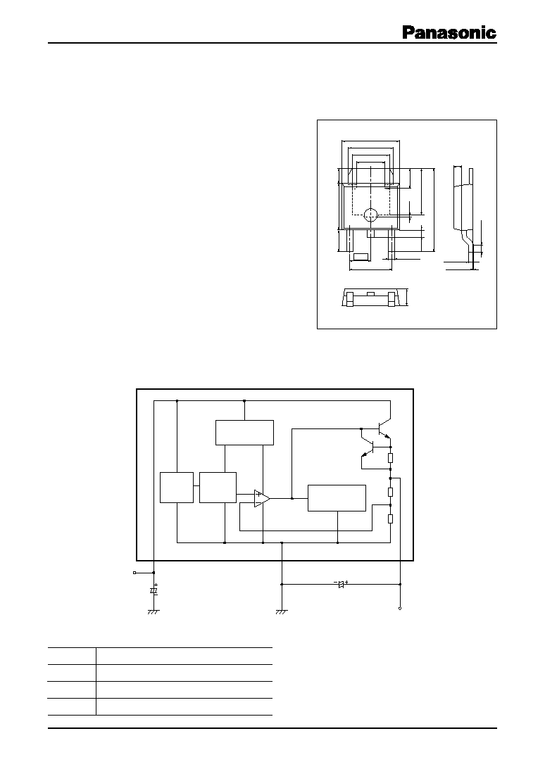
I Block Diagram
SP-3SU
Unit: mm
2.30
(3.00)
(4.35)
5.30±0.10
6.50±0.20
(1.80)
(0.20)
(0.80)
(2.50)
2.30±0.10
(5.50)
9.80±0.20
5.50±0.20
2.50
4.60±0.10
0.75±0.10
0.10±0.10
1.00±0.30
1
2
3
1.00±0.20
0.55
+0.10
≠0.05
Error amp.
Current
source
Voltage
reference
Starter
Pass Tr
Current
limitter
Thermal
protection
R2
R
SC
R1
1
Input
FIN
Output
C
O
C
I
C
I
0.33 µF, C
O
0.1 µF
2
3
I Pin Descriptions
Pin No.
Description
1
Input
Input voltage pin
2
GND
Ground pin (FIN)
3
Output
Output voltage pin
Note) The package of this product will be changed
to lead-free type (SP-3SUA). See the new pack-
age dimensions section later of this datasheet.
AN78xxNSP Series
2
SFF00011BEB
Note) 1. *1: Except for the operating ambient temperature and storage temperature, all ratings are for T
a
= 25∞C.
*2: The power dissipation shown is the value for the independent IC without a heat sink at T
a
= 85∞C.
When Tj exceeds 150
∞C (designed value), the internal circuit cuts off the output.
2. This IC is not suitable for car electronics equipment.
I Absolute Maximum Ratings
Parameter
Symbol
Range
Unit
Supply voltage
V
CC
35
V
Supply current
I
CC
mA
Power dissipation
*2
P
D
364
mW
Operating ambient temperature
*1
T
opr
-30 to +85
∞C
Storage temperature
*1
T
stg
-55 to +150
∞C
I Electrical Characteristics at T
a
= 25∞C
∑ AN7805NSP (5 V type)
The specified condition T
j
= 25∞C means that the test should be carried out within so short a test time (within 10 ms)
that the characteristic value drift due to the chip junction temperature rise can be ignored.
Unless otherwise specified, V
I
= 10 V, I
O
= 500 mA, C
I
= 0.33 µF and C
O
= 0.1 µF
Parameter
Symbol
Conditions
Min
Typ
Max
Unit
Output voltage
V
O1
T
j
= 25∞C
4.8
5
5.2
V
Output voltage tolerance
V
O2
V
I
= 8 V to 20 V, I
O
= 5 mA to 1 A
4.75
5.25
V
T
j
= 25∞C, P
D
< 5 W
Line regulation 1
REG
IN1
V
I
= 7.5 V to 25 V, T
j
= 25∞C
3
100
mV
Line regulation 2
REG
IN2
V
I
= 8 V to 12 V, T
j
= 25∞C
1
50
mV
Load regulation 1
REG
L1
I
O
= 5 mA to 1.5 A, T
j
= 25∞C
15
100
mV
Load regulation 2
REG
L2
I
O
= 250 mA to 750 mA, T
j
= 25∞C
5.0
50
mV
Bias current
I
Bias
T
j
= 25∞C
3.9
8
mA
Bias current fluctuation to input
I
Bias(IN)
V
I
= 7.5 V to 25 V, T
j
= 25∞C
1.3
mA
Bias current fluctuation to load
I
Bias(L)
I
O
= 5 mA to 1 A, T
j
= 25∞C
0.5
mA
Ripple rejection ratio
RR
V
I
= 8 V to 18 V, I
O
= 100 mA, f = 120 Hz
62
dB
∑ Design reference data
Note) The characteristics listed below are theoretical values based on the IC design and are not guaranteed.
Parameter
Symbol
Conditions
Min
Typ
Max
Unit
Output noise voltage
V
NO
f
= 10 Hz to 100 kHz
40
µV
Minimum input/output voltage V
DIF(min)
I
O
= 1 A, T
j
= 25∞C
2
V
difference
Output short-circuit current
I
O(Short)
V
I
= 35 V, T
j
= 25∞C
700
mA
Peak output current
I
O(Peak)
T
j
= 25∞C
2.0
A
Output voltage temperature
V
O
/ T
a
I
O
= 5 mA, T
j
= 0∞C to 125∞C
- 0.3
mV/
∞C
coefficient
Thermal protection operating
T
j(TH)
I
O
= 5 mA
150
∞C
temperature

AN78xxNSP Series
3
SFF00011BEB
I Electrical Characteristics at T
a
= 25∞C (continued)
∑ AN7806NSP (6 V type)
The specified condition T
j
= 25∞C means that the test should be carried out within so short a test time (within 10 ms)
that the characteristic value drift due to the chip junction temperature rise can be ignored.
Unless otherwise specified, V
I
= 11 V, I
O
= 500 mA, C
I
= 0.33 µF and C
O
= 0.1 µF
Parameter
Symbol
Conditions
Min
Typ
Max
Unit
Output noise voltage
V
NO
f
= 10 Hz to 100 kHz
40
µV
Minimum input/output voltage V
DIF(min)
I
O
= 1 A, T
j
= 25∞C
2
V
difference
Output short-circuit current
I
O(Short)
V
I
= 35 V, T
j
= 25∞C
700
mA
Peak output current
I
O(Peak)
T
j
= 25∞C
2.0
A
Output voltage temperature
V
O
/ T
a
I
O
= 5 mA, T
j
= 0∞C to 125∞C
- 0.4
mV/
∞C
coefficient
Thermal protection operating
T
j(TH)
I
O
= 5 mA
150
∞C
temperature
Parameter
Symbol
Conditions
Min
Typ
Max
Unit
Output voltage
V
O1
T
j
= 25∞C
5.75
6
6.25
V
Output voltage tolerance
V
O2
V
I
= 9 V to 21 V, I
O
= 5 mA to 1 A
5.7
6.3
V
T
j
= 25∞C, P
D
< 5 W
Line regulation 1
REG
IN1
V
I
= 8.5 V to 25 V, T
j
= 25∞C
5
120
mV
Line regulation 2
REG
IN2
V
I
= 9 V to 13 V, T
j
= 25∞C
1.5
60
mV
Load regulation 1
REG
L1
I
O
= 5 mA to 1.5 A, T
j
= 25∞C
14
120
mV
Load regulation 2
REG
L2
I
O
= 250 mA to 750 mA, T
j
= 25∞C
4.0
60
mV
Bias current
I
Bias
T
j
= 25∞C
3.9
8
mA
Bias current fluctuation to input
I
Bias(IN)
V
I
= 8.5 V to 25 V, T
j
= 25∞C
1.3
mA
Bias current fluctuation to load
I
Bias(L)
I
O
= 5 mA to 1 A, T
j
= 25∞C
0.5
mA
Ripple rejection ratio
RR
V
I
= 9 V to 19 V, I
O
= 100 mA, f = 120 Hz
59
dB
∑ Design reference data
Note) The characteristics listed below are theoretical values based on the IC design and are not guaranteed.
AN78xxNSP Series
4
SFF00011BEB
I Electrical Characteristics at T
a
= 25∞C (continued)
∑ AN7807NSP (7 V type)
The specified condition T
j
= 25∞C means that the test should be carried out within so short a test time (within 10 ms)
that the characteristic value drift due to the chip junction temperature rise can be ignored.
Unless otherwise specified, V
I
= 12 V, I
O
= 500 mA, C
I
= 0.33 µF and C
O
= 0.1 µF
Parameter
Symbol
Conditions
Min
Typ
Max
Unit
Output noise voltage
V
NO
f
= 10 Hz to 100 kHz
46
µV
Minimum input/output voltage V
DIF(min)
I
O
= 1 A, T
j
= 25∞C
2
V
difference
Output short-circuit current
I
O(Short)
V
I
= 35 V, T
j
= 25∞C
700
mA
Peak output current
I
O(Peak)
T
j
= 25∞C
2.0
A
Output voltage temperature
V
O
/ T
a
I
O
= 5 mA, T
j
= 0∞C to 125∞C
- 0.5
mV/
∞C
coefficient
Thermal protection operating
T
j(TH)
I
O
= 5 mA
150
∞C
temperature
Parameter
Symbol
Conditions
Min
Typ
Max
Unit
Output voltage
V
O1
T
j
= 25∞C
6.7
7
7.3
V
Output voltage tolerance
V
O2
V
I
= 10 V to 22 V, I
O
= 5 mA to 1 A
6.6
7.4
V
T
j
= 25∞C, P
D
< 5 W
Line regulation 1
REG
IN1
V
I
= 9.5 V to 25 V, T
j
= 25∞C
5
140
mV
Line regulation 2
REG
IN2
V
I
= 10 V to 15 V, T
j
= 25∞C
1.5
70
mV
Load regulation 1
REG
L1
I
O
= 5 mA to 1.5 A, T
j
= 25∞C
14
140
mV
Load regulation 2
REG
L2
I
O
= 250 mA to 750 mA, T
j
= 25∞C
4.0
70
mV
Bias current
I
Bias
T
j
= 25∞C
3.9
8
mA
Bias current fluctuation to input
I
Bias(IN)
V
I
= 9.5 V to 25 V, T
j
= 25∞C
1.0
mA
Bias current fluctuation to load
I
Bias(L)
I
O
= 5 mA to 1 A, T
j
= 25∞C
0.5
mA
Ripple rejection ratio
RR
V
I
= 10 V to 20 V, I
O
= 100 mA, f = 120 Hz
57
dB
∑ Design reference data
Note) The characteristics listed below are theoretical values based on the IC design and are not guaranteed.

AN78xxNSP Series
5
SFF00011BEB
I Electrical Characteristics at T
a
= 25∞C (continued)
∑ AN7808NSP (8 V type)
The specified condition T
j
= 25∞C means that the test should be carried out within so short a test time (within 10 ms)
that the characteristic value drift due to the chip junction temperature rise can be ignored.
Unless otherwise specified, V
I
= 14 V, I
O
= 500 mA, C
I
= 0.33 µF and C
O
= 0.1 µF
Parameter
Symbol
Conditions
Min
Typ
Max
Unit
Output noise voltage
V
NO
f
= 10 Hz to 100 kHz
52
µV
Minimum input/output voltage V
DIF(min)
I
O
= 1 A, T
j
= 25∞C
2
V
difference
Output short-circuit current
I
O(Short)
V
I
= 35 V, T
j
= 25∞C
700
mA
Peak output current
I
O(Peak)
T
j
= 25∞C
2.0
A
Output voltage temperature
V
O
/ T
a
I
O
= 5 mA, T
j
= 0∞C to 125∞C
- 0.5
mV/
∞C
coefficient
Thermal protection operating
T
j(TH)
I
O
= 5 mA
150
∞C
temperature
Parameter
Symbol
Conditions
Min
Typ
Max
Unit
Output voltage
V
O1
T
j
= 25∞C
7.7
8
8.3
V
Output voltage tolerance
V
O2
V
I
= 11 V to 23 V, I
O
= 5 mA to 1 A
7.6
8.4
V
T
j
= 25∞C, P
D
< 5 W
Line regulation 1
REG
IN1
V
I
= 10.5 V to 25 V, T
j
= 25∞C
6
160
mV
Line regulation 2
REG
IN2
V
I
= 11 V to 17 V, T
j
= 25∞C
2
80
mV
Load regulation 1
REG
L1
I
O
= 5 mA to 1.5 A, T
j
= 25∞C
12
160
mV
Load regulation 2
REG
L2
I
O
= 250 mA to 750 mA, T
j
= 25∞C
4.0
80
mV
Bias current
I
Bias
T
j
= 25∞C
3.9
8
mA
Bias current fluctuation to input
I
Bias(IN)
V
I
= 10.5 V to 25 V, T
j
= 25∞C
1.0
mA
Bias current fluctuation to load
I
Bias(L)
I
O
= 5 mA to 1 A, T
j
= 25∞C
0.5
mA
Ripple rejection ratio
RR
V
I
= 11.5 V to 21.5 V, I
O
= 100 mA, f = 120 Hz 56
dB
∑ Design reference data
Note) The characteristics listed below are theoretical values based on the IC design and are not guaranteed.

AN78xxNSP Series
6
SFF00011BEB
I Electrical Characteristics at T
a
= 25∞C (continued)
∑ AN7809NSP (9 V type)
The specified condition T
j
= 25∞C means that the test should be carried out within so short a test time (within 10 ms)
that the characteristic value drift due to the chip junction temperature rise can be ignored.
Unless otherwise specified, V
I
= 15 V, I
O
= 500 mA, C
I
= 0.33 µF and C
O
= 0.1 µF
Parameter
Symbol
Conditions
Min
Typ
Max
Unit
Output noise voltage
V
NO
f
= 10 Hz to 100 kHz
57
µV
Minimum input/output voltage V
DIF(min)
I
O
= 1 A, T
j
= 25∞C
2
V
difference
output short-circuit current
I
O(Short)
V
I
= 35 V, T
j
= 25∞C
700
mA
Peak output current
I
O(Peak)
T
j
= 25∞C
2.0
A
Output voltage temperature
V
O
/ T
a
I
O
= 5 mA, T
j
= 0∞C to 125∞C
- 0.5
mV/
∞C
coefficient
Thermal protection operating
T
j(TH)
I
O
= 5 mA
150
∞C
temperature
Parameter
Symbol
Conditions
Min
Typ
Max
Unit
Output voltage
V
O1
T
j
= 25∞C
8.65
9
9.35
V
Output voltage tolerance
V
O2
V
I
= 12 V to 24 V, I
O
= 5 mA to 1 A
8.55
9.45
V
T
j
= 25∞C, P
D
< 5 W
Line regulation 1
REG
IN1
V
I
= 11.5 V to 26 V, T
j
= 25∞C
7
180
mV
Line regulation 2
REG
IN2
V
I
= 12 V to 18 V, T
j
= 25∞C
2
90
mV
Load regulation 1
REG
L1
I
O
= 5 mA to 1.5 A, T
j
= 25∞C
12
180
mV
Load regulation 2
REG
L2
I
O
= 250 mA to 750 mA, T
j
= 25∞C
4.0
90
mV
Bias current
I
Bias
T
j
= 25∞C
3.9
8
mA
Bias current fluctuation to input
I
Bias(IN)
V
I
= 11.5 V to 26 V, T
j
= 25∞C
1.0
mA
Bias current fluctuation to load
I
Bias(L)
I
O
= 5 mA to 1 A, T
j
= 25∞C
0.5
mA
Ripple rejection ratio
RR
V
I
= 11.5 V to 21.5 V, I
O
= 100 mA, f = 120 Hz 56
dB
∑ Design reference data
Note) The characteristics listed below are theoretical values based on the IC design and are not guaranteed.
AN78xxNSP Series
7
SFF00011BEB
I Electrical Characteristics at T
a
= 25∞C (continued)
∑ AN7810NSP (10 V type)
The specified condition T
j
= 25∞C means that the test should be carried out within so short a test time (within 10 ms)
that the characteristic value drift due to the chip junction temperature rise can be ignored.
Unless otherwise specified, V
I
= 16 V, I
O
= 500 mA, C
I
= 0.33 µF and C
O
= 0.1 µF
Parameter
Symbol
Conditions
Min
Typ
Max
Unit
Output noise voltage
V
NO
f
= 10 Hz to 100 kHz
56
µV
Minimum input/output voltage V
DIF(min)
I
O
= 1 A, T
j
= 25∞C
2
V
difference
Output short-circuit current
I
O(Short)
V
I
= 35 V, T
j
= 25∞C
700
mA
Peak output current
I
O(Peak)
T
j
= 25∞C
2.0
A
Output voltage temperature
V
O
/ T
a
I
O
= 5 mA, T
j
= 0∞C to 125∞C
- 0.6
mV/
∞C
coefficient
Thermal protection operating
T
j(TH)
I
O
= 5 mA
150
∞C
temperature
Parameter
Symbol
Conditions
Min
Typ
Max
Unit
Output voltage
V
O1
T
j
= 25∞C
9.6
10
10.4
V
Output voltage tolerance
V
O2
V
I
= 13 V to 25 V, I
O
= 5 mA to 1 A
9.5
10.5
V
T
j
= 25∞C, P
D
< 5 W
Line regulation 1
REG
IN1
V
I
= 12.5 V to 27 V, T
j
= 25∞C
8
200
mV
Line regulation 2
REG
IN2
V
I
= 13 V to 19 V, T
j
= 25∞C
2.5
100
mV
Load regulation 1
REG
L1
I
O
= 5 mA to 1.5 A, T
j
= 25∞C
12
200
mV
Load regulation 2
REG
L2
I
O
= 250 mA to 750 mA, T
j
= 25∞C
4.0
100
mV
Bias current
I
Bias
T
j
= 25∞C
3.9
8
mA
Bias current fluctuation to input
I
Bias(IN)
V
I
= 12.5 V to 27 V, T
j
= 25∞C
1.0
mA
Bias current fluctuation to load
I
Bias(L)
I
O
= 5 mA to 1 A, T
j
= 25∞C
0.5
mA
Ripple rejection ratio
RR
V
I
= 13 V to 23 V, I
O
= 100 mA, f = 120 Hz
56
dB
∑ Design reference data
Note) The characteristics listed below are theoretical values based on the IC design and are not guaranteed.

AN78xxNSP Series
8
SFF00011BEB
I Electrical Characteristics at T
a
= 25∞C (continued)
∑ AN7812NSP (12 V type)
The specified condition T
j
= 25∞C means that the test should be carried out within so short a test time (within 10 ms)
that the characteristic value drift due to the chip junction temperature rise can be ignored.
Unless otherwise specified, V
I
= 19 V, I
O
= 500 mA, C
I
= 0.33 µF and C
O
= 0.1 µF
Parameter
Symbol
Conditions
Min
Typ
Max
Unit
Output noise voltage
V
NO
f
= 10 Hz to 100 kHz
75
µV
Minimum input/output voltage V
DIF(min)
I
O
= 1 A, T
j
= 25∞C
2
V
difference
Output short-circuit current
I
O(Short)
V
I
= 35 V, T
j
= 25∞C
700
mA
Peak output current
I
O(Peak)
T
j
= 25∞C
2.0
A
Output voltage temperature
V
O
/ T
a
I
O
= 5 mA, T
j
= 0∞C to 125∞C
- 0.8
mV/
∞C
coefficient
Thermal protection operating
T
j(TH)
I
O
= 5 mA
150
∞C
temperature
Parameter
Symbol
Conditions
Min
Typ
Max
Unit
Output voltage
V
O1
T
j
= 25∞C
11.5
12
12.5
V
Output voltage tolerance
V
O2
V
I
= 15 V to 27 V, I
O
= 5 mA to 1 A
11.4
12.6
V
T
j
= 25∞C, P
D
< 5 W
Line regulation 1
REG
IN1
V
I
= 14.5 V to 30 V, T
j
= 25∞C
10
240
mV
Line regulation 2
REG
IN2
V
I
= 16 V to 22 V, T
j
= 25∞C
2
120
mV
Load regulation 1
REG
L1
I
O
= 5 mA to 1.5 A, T
j
= 25∞C
12
240
mV
Load regulation 2
REG
L2
I
O
= 250 mA to 750 mA, T
j
= 25∞C
4.0
120
mV
Bias current
I
Bias
T
j
= 25∞C
4.0
8
mA
Bias current fluctuation to input
I
Bias(IN)
V
I
= 14.5 V to 30 V, T
j
= 25∞C
1.0
mA
Bias current fluctuation to load
I
Bias(L)
I
O
= 5 mA to 1 A, T
j
= 25∞C
0.5
mA
Ripple rejection ratio
RR
V
I
= 15 V to 25 V, I
O
= 100 mA, f = 120 Hz
55
dB
∑ Design reference data
Note) The characteristics listed below are theoretical values based on the IC design and are not guaranteed.

AN78xxNSP Series
9
SFF00011BEB
I Electrical Characteristics at T
a
= 25∞C (continued)
∑ AN7815NSP (15 V type)
The specified condition T
j
= 25∞C means that the test should be carried out within so short a test time (within 10 ms)
that the characteristic value drift due to the chip junction temperature rise can be ignored.
Unless otherwise specified, V
I
= 23 V, I
O
= 500 mA, C
I
= 0.33 µF and C
O
= 0.1 µF
Parameter
Symbol
Conditions
Min
Typ
Max
Unit
Output noise voltage
V
NO
f
= 10 Hz to 100 kHz
90
µV
Minimum input/output voltage V
DIF(min)
I
O
= 1 A, T
j
= 25∞C
2
V
difference
Output short-circuit current
I
O(Short)
V
I
= 35 V, T
j
= 25∞C
700
mA
Peak output current
I
O(Peak)
T
j
= 25∞C
2.0
A
Output voltage temperature
V
O
/ T
a
I
O
= 5 mA, T
j
= 0∞C to 125∞C
-1.0
mV/
∞C
coefficient
Thermal protection operating
T
j(TH)
I
O
= 5 mA
150
∞C
temperature
Parameter
Symbol
Conditions
Min
Typ
Max
Unit
Output voltage
V
O1
T
j
= 25∞C
14.4
15
15.6
V
Output voltage tolerance
V
O2
V
I
= 18 V to 30 V, I
O
= 5 mA to 1 A
14.25
15.75
V
T
j
= 25∞C, P
D
< 5 W
Line regulation 1
REG
IN1
V
I
= 17.5 V to 30 V, T
j
= 25∞C
11
300
mV
Line regulation 2
REG
IN2
V
I
= 20 V to 26 V, T
j
= 25∞C
3
150
mV
Load regulation 1
REG
L1
I
O
= 5 mA to 1.5 A, T
j
= 25∞C
12
300
mV
Load regulation 2
REG
L2
I
O
= 250 mA to 750 mA, T
j
= 25∞C
4.0
150
mV
Bias current
I
Bias
T
j
= 25∞C
4.0
8
mA
Bias current fluctuation to input
I
Bias(IN)
V
I
= 17.5 V to 30 V, T
j
= 25∞C
1.0
mA
Bias current fluctuation to load
I
Bias(L)
I
O
= 5 mA to 1 A, T
j
= 25∞C
0.5
mA
Ripple rejection ratio
RR
V
I
= 18.5 V to 28.5 V, I
O
= 100 mA, f = 120 Hz 54
dB
∑ Design reference data
Note) The characteristics listed below are theoretical values based on the IC design and are not guaranteed.

AN78xxNSP Series
10
SFF00011BEB
I Electrical Characteristics at T
a
= 25∞C (continued)
∑ AN7818NSP (18 V type)
The specified condition T
j
= 25∞C means that the test should be carried out within so short a test time (within 10 ms)
that the characteristic value drift due to the chip junction temperature rise can be ignored.
Unless otherwise specified, V
I
= 27 V, I
O
= 500 mA, C
I
= 0.33 µF and C
O
= 0.1 µF
Parameter
Symbol
Conditions
Min
Typ
Max
Unit
Output noise voltage
V
NO
f
= 10 Hz to 100 kHz
110
µV
Minimum input/output voltage V
DIF(min)
I
O
= 1 A, T
j
= 25∞C
2
V
difference
Output short-circuit current
I
O(Short)
V
I
= 35 V, T
j
= 25∞C
700
mA
Peak output current
I
O(Peak)
T
j
= 25∞C
2.0
A
Output voltage temperature
V
O
/ T
a
I
O
= 5 mA, T
j
= 0∞C to 125∞C
-1.1
mV/
∞C
coefficient
Thermal protection operating
T
j(TH)
I
O
= 5 mA
150
∞C
temperature
Parameter
Symbol
Conditions
Min
Typ
Max
Unit
Output voltage
V
O1
T
j
= 25∞C
17.3
18
18.7
V
Output voltage tolerance
V
O2
V
I
= 21 V to 33 V, I
O
= 5 mA to 1 A
17.1
18.9
V
T
j
= 25∞C, P
D
< 5 W
Line regulation 1
REG
IN1
V
I
= 21 V to 33 V, T
j
= 25∞C
14
360
mV
Line regulation 2
REG
IN2
V
I
= 24 V to 30 V, T
j
= 25∞C
4
180
mV
Load regulation 1
REG
L1
I
O
= 5 mA to 1.5 A, T
j
= 25∞C
14
360
mV
Load regulation 2
REG
L2
I
O
= 250 mA to 750 mA, T
j
= 25∞C
4.0
180
mV
Bias current
I
Bias
T
j
= 25∞C
4.1
8
mA
Bias current fluctuation to input
I
Bias(IN)
V
I
= 21 V to 33 V, T
j
= 25∞C
1.0
mA
Bias current fluctuation to load
I
Bias(L)
I
O
= 5 mA to 1 A, T
j
= 25∞C
0.5
mA
Ripple rejection ratio
RR
V
I
= 22 V to 32 V, I
O
= 100 mA, f = 120 Hz
53
dB
∑ Design reference data
Note) The characteristics listed below are theoretical values based on the IC design and are not guaranteed.

AN78xxNSP Series
11
SFF00011BEB
5.00
6.00
0
25
150
50
75
100
125
4.00
3.00
2.00
0.85
0.70
1.00
1.40
0
Mounted on
glass epoxy board 2
(50
◊ 50 ◊ t1.5 mm
3
)
R
th(j-a)
= 89.3∞C/W
Mounted on
glass epoxy board 1
(20
◊ 20 ◊ t1.7 mm
3
)
R
th(j-a)
= 147.0∞C/W
Independent IC
without a heat sink
R
th( j-a)
= 178.0∞C/W
Mounted on Al board
(50
◊ 50 ◊ t2.0 mm
3
)
R
th(j-a)
= 25.0∞C/W
Ambient temperature
T
a
(
∞C)
Power dissipation
P
D
(W
)
I Application Notes
1. P
D
T
a
curves of SP-3SU
P
D
T
a
2. Main Characteristics
Minimum input/output voltage difference vs.
Minimum input/output voltage difference
load current characteristic
temperature characteristic
Peak output current temperature characteristic
Current limit characteristics
V
DIF
(V)
1
0
0.8
0.6
0.4
0.2
I
O
(A)
0
0.2
0.4
0.6
0.8
1.0
1.2
1.4
1.6
1.8
2
T
j
= 25∞C
I
O(Peak)
(A)
120
-40
80
40
0
-20
100
60
20
T
a
(
∞C)
0.000
2.500
0.500
1.000
1.500
2.000
V
DIF(min)
(V)
1.800
1.820
1.840
1.860
1.880
1.900
1.920
1.940
1.960
1.980
2.000
120
-40
80
40
0
-20
100
60
20
T
a
(
∞C)
I
O
= -1 A
V
O
(V)
2
1.5
1
0
0.5
I
O
(A)
0
6
1
2
3
4
5
V
I
= 10 V
V
I
= 20 V
V
I
= 30 V
T
j
= 25∞C

AN78xxNSP Series
12
SFF00011BEB
I New Package Dimensions (Unit: mm)
∑ SP-3SUA (Lead-free package)
3
2
1
(0.50)
(2.50)
(5.30)
(1.80)
6.50
±0.10
(4.35)
(3.00)
5.40
±0.10
1.00
±
0.20
0.10
±0.10
2.30
±
0.10
0.75
+0.10
-0.05
0.50
+0.10
-0.05
1.00
±0.20
2.50
±
0.20
4.60
±0.10
(0.50)
9.80
±
0.20
5.50
±
0.10
2.30
M
0.23

Please read the following notes before using the datasheets
A. These materials are intended as a reference to assist customers with the selection of Panasonic
semiconductor products best suited to their applications.
Due to modification or other reasons, any information contained in this material, such as available
product types, technical data, and so on, is subject to change without notice.
Customers are advised to contact our semiconductor sales office and obtain the latest information
before starting precise technical research and/or purchasing activities.
B. Panasonic is endeavoring to continually improve the quality and reliability of these materials but
there is always the possibility that further rectifications will be required in the future. Therefore,
Panasonic will not assume any liability for any damages arising from any errors etc. that may ap-
pear in this material.
C. These materials are solely intended for a customer's individual use.
Therefore, without the prior written approval of Panasonic, any other use such as reproducing,
selling, or distributing this material to a third party, via the Internet or in any other way, is prohibited.
Request for your special attention and precautions in using the technical information
and semiconductors described in this material
(1) An export permit needs to be obtained from the competent authorities of the Japanese Govern-
ment if any of the products or technologies described in this material and controlled under the
"Foreign Exchange and Foreign Trade Law" is to be exported or taken out of Japan.
(2) The technical information described in this material is limited to showing representative character-
istics and applied circuit examples of the products. It does not constitute the warranting of industrial
property, the granting of relative rights, or the granting of any license.
(3) The products described in this material are intended to be used for standard applications or gen-
eral electronic equipment (such as office equipment, communications equipment, measuring in-
struments and household appliances).
Consult our sales staff in advance for information on the following applications:
∑ Special applications (such as for airplanes, aerospace, automobiles, traffic control equipment,
combustion equipment, life support systems and safety devices) in which exceptional quality and
reliability are required, or if the failure or malfunction of the products may directly jeopardize life or
harm the human body.
∑ Any applications other than the standard applications intended.
(4) The products and product specifications described in this material are subject to change without
notice for reasons of modification and/or improvement. At the final stage of your design, purchas-
ing, or use of the products, therefore, ask for the most up-to-date Product Standards in advance to
make sure that the latest specifications satisfy your requirements.
(5) When designing your equipment, comply with the guaranteed values, in particular those of maxi-
mum rating, the range of operating power supply voltage and heat radiation characteristics. Other-
wise, we will not be liable for any defect which may arise later in your equipment.
Even when the products are used within the guaranteed values, redundant design is recommended,
so that such equipment may not violate relevant laws or regulations because of the function of our
products.
(6) When using products for which dry packing is required, observe the conditions (including shelf life
and after-unpacking standby time) agreed upon when specification sheets are individually exchanged.
(7) No part of this material may be reprinted or reproduced by any means without written permission
from our company.
2001 MAR