 | –≠–ª–µ–∫—Ç—Ä–æ–Ω–Ω—ã–π –∫–æ–º–ø–æ–Ω–µ–Ω—Ç: AN78L00M | –°–∫–∞—á–∞—Ç—å:  PDF PDF  ZIP ZIP |
s Overview
The AN78L00 series is 3-pin fixed positive output type
monolithic voltage regulators.
A Stabilized fixed output voltage is obtained from an
unstable DC input voltage without using any external
parts. Eleven types of fixed output voltage are available
from 4V through 10V, 12V, 15V, 18V, 20V, and 24V. They
can be used widely as power circuits with a current
capacitance of up to 100mA.
s Features
∑ No external components
∑ Output voltage:4V, 5V, 6V, 7V, 8V, 9V, 10V, 12V,
15V, 18V, 20V, 24V
∑ Internal short-circuit current limiting
∑ Internal thermal overload protection
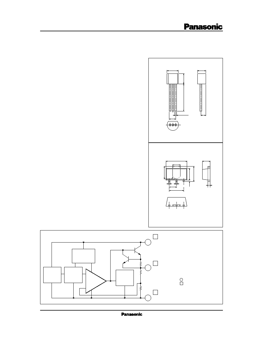
AN78L00/AN78L00M Series
3-pin Positive Output Voltage Regulator (100mA Type)
s Block Diagram
Unit:mm
AN78L00 Series
5.0
±
0.2
TO-92 Package (SSIP003-P-0000)
5.1
±
0.2
13.5
±
0.5
0.45
2.3
±
0.2
1:Input
2:Output
3:Common
2.54
(Bottom View)
3
2
1
+ 0.2
≠ 0.1
4.0
±
0.2
1:Output
2:Common
3:Input
0.44max.
AN78L00M Series
Unit:mm
3-pin SIL Mini Power Type Plastic Package (HSIP003-P-0000B)
4.6max.
1.6max.
0.48max.
1.8max.
1.5
3.0
2.6max.
4.25max.
0.8min.
2.6
0.58max.
4.5
1
2
3
1
2
3
Input
Pass Tr
Output
Common
Starter
Voltage
Reference
Current
Source
Error Amp.
+
≠
Thermal
Protection
Q
1
R
SC
R
2
R
1
Current
Limiter
3
1
2
Pin Number in are for AN78L00 Series
Pin Number in are for AN78L00M Series
V
I
P
D
T
opr
T
stg
V
V
mW
∞C
∞C
Parameter
Symbol
Rating
Unit
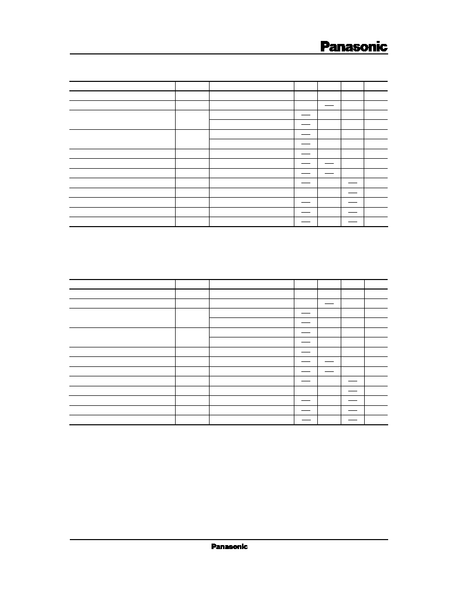
s Absolute Maximum Ratings (Ta=25∞C)
35 *
1
40 *
2
650 *
3
≠30 to +80
≠55 to +150
≠55 to +125
Input voltage
Power dissipation
Operating ambient temperature
Storage temperature
AN78L00 Series
AN78L00M Series
*1 AN78L04/M, AN78L05/M, AN78L06/M, AN78L07/M, AN78L08/M, AN78L09/M, AN78L10/M, AN78L12/M, AN78L15/M
*2 AN78L18/M, AN78L20/M, AN78L24/M
*3 Follow the derating curve. When T
j
exceeds 150∞C, the internal circuit shuts off the output.
Mounting onto the PCB (20
◊
20
◊
1.7mm glass epoxy copper foil 1cm
2
or more), for AN78L00M Series.
V
O
4.16
V
4
T
j
=25∞C
V
O
V
V
I
=6.5 to 19V, I
O
=1 to 70mA
REG
IN
145
mV
50
V
I
=6.5 to 19V, T
j
=25∞C
mV
REG
L
mV
10
I
O
=1 to 100mA, T
j
=25∞C
mV
I
O
=1 to 40mA, T
j
=25∞C
V
I
=7 to 19V, T
j
=25∞C
mA
2
T
j
=25∞C
40
I
bias
mA
V
I
=7 to 19V, T
j
=25∞C
mA
40
I
O
=1 to 40mA, T
j
=25∞C
V
no
dB
f=10Hz to 100kHz
1
0.1
95
4.2
55
30
3
48
3.84
3.8
RR
V
I
=7 to 17V, I
O
=40mA, f=120Hz
V
1.7
T
j
=25∞C
mA
140
≠ 0.6
T
j
=25∞C, V
I
=35V
4.5
58
I
O
=5mA, T
j
=0 to 125∞C
Parameter
Symbol
Condition
min
typ
max
Output voltage
Output voltage tolerance
Line regulation
Load regulation
Note 1) The specified condition T
j
=25∞C means that the test should be conducted with each test time reducedt (within 10ms) so that
the drift in characteristic value due to a temperature rise at chip junction can be innored.
Note 2) Unless otherwise specified, V
I
=9V, I
O
=40mA, C
I
=0.33
µ
F, C
O
=0.1
µ
F, T
j
=0 to 125∞C (AN78L04) and T
j
=0 to 100∞C
(AN78L04M).
Bias current
Input bias current fluctuation
Load bias current fluctuation
Output noise voltage
Ripple rejection ratio
Minimum I/O voltage difference
Output short-circuit current
Output voltage temperature cofficient
Unit
s Electrical Characteristics (Ta=25∞C)
∑
AN78L04/AN78L04M (4V Type)
I
bias (IN)
I
bias (L)
V
DIF (min.)
I
O (Short)
V
O
/Ta
µ
V
mV/∞C
V
O
5.2
V
5
T
j
=25∞C
V
O
V
V
I
=7.5 to 20V, I
O
=1 to 70mA
REG
IN
150
mV
55
V
I
=7.5 to 20V, T
j
=25∞C
mV
REG
L
mV
11
I
O
=1 to 100mA, T
j
=25∞C
mV
I
O
=1 to 40mA, T
j
=25∞C
V
I
=8 to 20V, T
j
=25∞C
mA
2
T
j
=25∞C
45
I
bias
mA
V
I
=8 to 20V, T
j
=25∞C
mA
40
I
O
=1 to 40mA, T
j
=25∞C
V
no
dB
f=10Hz to 100kHz
1
0.1
100
5.25
60
30
3
47
4.8
4.75
RR
V
I
=8 to 18V, I
O
=40mA, f=120Hz
V
1.7
T
j
=25∞C
mA
140
≠ 0.65
T
j
=25∞C, V
I
=35V
5
57
I
O
=5mA, T
j
=0 to 125∞C
Parameter
Symbol
Condition
min
typ
max
Output voltage
Output voltage tolerance
Line regulation
Load regulation
Bias current
Input bias current fluctuation
Load bias current fluctuation
Output noise voltage
Ripple rejection ratio
Minimum I/O voltage difference
Output short-circuit current
Output voltage temperature cofficient
Unit
Note 1) The specified condition T
j
=25∞C means that the test should be conducted with each test time reducedt (within 10ms) so that
the drift in characteristic value due to a temperature rise at chip junction can be innored.
Note 2) Unless otherwise specified, V
I
=10V, I
O
=40mA, C
I
=0.33
µ
F, C
O
=0.1
µ
F, T
j
=0 to 125∞C (AN78L05) and T
j
=0 to 100∞C
(AN78L05M).
s Electrical Characteristics (Ta=25∞C)
∑
AN78L05/AN78L05M (5V Type)
I
bias (IN)
I
bias (L)
V
DIF (min.)
I
O (Short)
V
O
/Ta
µ
V
mV/∞C
V
O
6.24
V
6
T
j
=25∞C
V
O
V
V
I
=8.5 to 21V, I
O
=1 to 70mA
REG
IN
155
mV
60
V
I
=8.5 to 21V, T
j
=25∞C
mV
REG
L
mV
12
I
O
=1 to 100mA, T
j
=25∞C
mV
I
O
=1 to 40mA, T
j
=25∞C
V
I
=9 to 21V, T
j
=25∞C
mA
2
T
j
=25∞C
50
I
bias
mA
V
I
=9 to 21V, T
j
=25∞C
mA
50
I
O
=1 to 40mA, T
j
=25∞C
V
no
dB
f=10Hz to 100kHz
1
0.1
105
6.3
65
35
3
46
5.76
5.7
RR
V
I
=9 to 19V, I
O
=40mA, f=120Hz
V
1.7
T
j
=25∞C
mA
140
≠ 0.7
T
j
=25∞C, V
I
=35V
5.5
56
I
O
=5mA, T
j
=0 to 125∞C
Parameter
Symbol
Condition
min
typ
max
Output voltage
Output voltage tolerance
Line regulation
Load regulation
Bias current
Input bias current fluctuation
Load bias current fluctuation
Output noise voltage
Ripple rejection ratio
Minimum I/O voltage difference
Output short-circuit current
Output voltage temperature cofficient
Unit
Note 1) The specified condition T
j
=25∞C means that the test should be conducted with each test time reducedt (within 10ms) so that
the drift in characteristic value due to a temperature rise at chip junction can be innored.
Note 2) Unless otherwise specified, V
I
=11V, I
O
=40mA, C
I
=0.33
µ
F, C
O
=0.1
µ
F, T
j
=0 to 125∞C (AN78L06) and T
j
=0 to 100∞C
(AN78L06M).
∑
AN78L06/AN78L06M (6V Type)
I
bias (IN)
I
bias (L)
V
DIF (min.)
I
O (Short)
V
O
/Ta
µ
V
mV/∞C
V
O
7.28
V
7
T
j
=25∞C
V
O
V
V
I
=9.5 to 22V, I
O
=1 to 70mA
REG
IN
165
mV
70
V
I
=9.5 to 22V, T
j
=25∞C
mV
REG
L
mV
13
I
O
=1 to 100mA, T
j
=25∞C
mV
I
O
=1 to 40mA, T
j
=25∞C
V
I
=10 to 22V, T
j
=25∞C
mA
2
T
j
=25∞C
60
I
bias
mA
V
I
=10 to 22V, T
j
=25∞C
mA
50
I
O
=1 to 40mA, T
j
=25∞C
V
no
dB
f=10Hz to 100kHz
1
0.1
115
7.35
75
35
3
45
6.72
6.65
RR
V
I
=10 to 20V, I
O
=40mA, f=120Hz
V
1.7
T
j
=25∞C
mA
140
≠ 0.75
T
j
=25∞C, V
I
=35V
6
55
I
O
=5mA, T
j
=0 to 125∞C
Parameter
Symbol
Condition
min
typ
max
Output voltage
Output voltage tolerance
Line regulation
Load regulation
Bias current
Input bias current fluctuation
Load bias current fluctuation
Output noise voltage
Ripple rejection ratio
Minimum I/O voltage difference
Output short-circuit current
Output voltage temperature cofficient
Unit
Note 1) The specified condition T
j
=25∞C means that the test should be conducted with each test time reducedt (within 10ms) so that
the drift in characteristic value due to a temperature rise at chip junction can be innored.
Note 2) Unless otherwise specified, V
I
=12V, I
O
=40mA, C
I
=0.33
µ
F, C
O
=0.1
µ
F, T
j
=0 to 125∞C (AN78L07) and T
j
=0 to 100∞C
(AN78L07M).
s Electrical Characteristics (Ta=25∞C)
∑
AN78L07/AN78L07M (7V Type)
I
bias (IN)
I
bias (L)
V
DIF (min.)
I
O (Short)
V
O
/Ta
µ
V
mV/∞C
V
O
8.3
V
8
T
j
=25∞C
V
O
V
V
I
=10.5 to 23V, I
O
=1 to 70mA
REG
IN
175
mV
80
V
I
=10.5 to 23V, T
j
=25∞C
mV
REG
L
mV
15
I
O
=1 to 100mA, T
j
=25∞C
mV
I
O
=1 to 40mA, T
j
=25∞C
V
I
=11 to 23V, T
j
=25∞C
mA
2
T
j
=25∞C
70
I
bias
mA
V
I
=11 to 23V, T
j
=25∞C
mA
60
I
O
=1 to 40mA, T
j
=25∞C
V
no
dB
f=10Hz to 100kHz
1
0.1
125
8.4
80
40
3
44
7.7
7.6
RR
V
I
=11 to 21V, I
O
=40mA, f=120Hz
V
1.7
T
j
=25∞C
mA
140
≠ 0.8
T
j
=25∞C, V
I
=35V
7
54
I
O
=5mA, T
j
=0 to 125∞C
Parameter
Symbol
Condition
min
typ
max
Output voltage
Output voltage tolerance
Line regulation
Load regulation
Bias current
Input bias current fluctuation
Load bias current fluctuation
Output noise voltage
Ripple rejection ratio
Minimum I/O voltage difference
Output short-circuit current
Output voltage temperature cofficient
Unit
Note 1) The specified condition T
j
=25∞C means that the test should be conducted with each test time reducedt (within 10ms) so that
the drift in characteristic value due to a temperature rise at chip junction can be innored.
Note 2) Unless otherwise specified, V
I
=14V, I
O
=40mA, C
I
=0.33
µ
F, C
O
=0.1
µ
F, T
j
=0 to 125∞C (AN78L08) and T
j
=0 to 100∞C
(AN78L08M).
∑
AN78L08/AN78L08M (8V Type)
I
bias (IN)
I
bias (L)
V
DIF (min.)
I
O (Short)
V
O
/Ta
µ
V
mV/∞C
V
O
9.35
V
9
T
j
=25∞C
V
O
V
V
I
=11.5 to 24V, I
O
=1 to 70mA
REG
IN
190
mV
90
V
I
=11.5 to 24V, T
j
=25∞C
mV
REG
L
mV
16
I
O
=1 to 100mA, T
j
=25∞C
mV
I
O
=1 to 40mA, T
j
=25∞C
V
I
=12 to 24V, T
j
=25∞C
mA
2
T
j
=25∞C
80
I
bias
mA
V
I
=12 to 24V, T
j
=25∞C
mA
65
I
O
=1 to 40mA, T
j
=25∞C
V
no
dB
f=10Hz to 100kHz
1
0.1
140
9.45
85
45
3
43
8.64
8.55
RR
V
I
=12 to 22V, I
O
=40mA, f=120Hz
V
1.7
T
j
=25∞C
mA
140
≠ 0.85
T
j
=25∞C , V
I
=35V
8
53
I
O
=5mA, T
j
=0 to 125∞C
Parameter
Symbol
Condition
min
typ
max
Output voltage
Output voltage tolerance
Line regulation
Load regulation
Bias current
Input bias current fluctuation
Load bias current fluctuation
Output noise voltage
Ripple rejection ratio
Minimum I/O voltage difference
Output short-circuit current
Output voltage temperature cofficient
Unit
Note 1) The specified condition T
j
=25∞C means that the test should be conducted with each test time reducedt (within 10ms) so that
the drift in characteristic value due to a temperature rise at chip junction can be innored.
Note 2) Unless otherwise specified, V
I
=15V, I
O
=40mA, C
I
=0.33
µ
F, C
O
=0.1
µ
F, T
j
=0 to 125∞C (AN78L09) and T
j
=0 to 100∞C
(AN78L09M).
s Electrical Characteristics (Ta=25∞C)
∑
AN78L09/AN78L09M (9V Type)
I
bias (IN)
I
bias (L)
V
DIF (min.)
I
O (Short)
V
O
/Ta
µ
V
mV/∞C
V
O
10.4
V
10
T
j
=25∞C
V
O
V
V
I
=12.5 to 25V, I
O
=1 to 70mA
REG
IN
210
mV
100
V
I
=12.5 to 25V, T
j
=25∞C
mV
REG
L
mV
17
I
O
=1 to 100mA, T
j
=25∞C
mV
I
O
=1 to 40mA, T
j
=25∞C
V
I
=13 to 25V, T
j
=25∞C
mA
2
T
j
=25∞C
90
I
bias
mA
V
I
=13 to 25V, T
j
=25∞C
mA
70
I
O
=1 to 40mA, T
j
=25∞C
V
no
dB
f=10Hz to 100kHz
1
0.1
160
10.5
90
45
3
42
9.6
9.5
RR
V
I
=13 to 23V, I
O
=40mA, f=120Hz
V
1.7
T
j
=25∞C
mA
140
≠ 0.9
T
j
=25∞C, V
I
=35V
9
52
I
O
=5mA, T
j
=0 to 125∞C
Parameter
Symbol
Condition
min
typ
max
Output voltage
Output voltage tolerance
Line regulation
Load regulation
Bias current
Input bias current fluctuation
Load bias current fluctuation
Output noise voltage
Ripple rejection ratio
Minimum I/O voltage difference
Output short-circuit current
Output voltage temperature cofficient
Unit
Note 1) The specified condition T
j
=25∞C means that the test should be conducted with each test time reducedt (within 10ms) so that
the drift in characteristic value due to a temperature rise at chip junction can be innored.
Note 2) Unless otherwise specified, V
I
=16V, I
O
=40mA, C
I
=0.33
µ
F, C
O
=0.1
µ
F, T
j
=0 to 125∞C (AN78L10) and T
j
=0 to 100∞C
(AN78L10M).
∑
AN78L10/AN78L10M (10V Type)
I
bias (IN)
I
bias (L)
V
DIF (min.)
I
O (Short)
V
O
/Ta
µ
V
mV/∞C