 | –≠–ª–µ–∫—Ç—Ä–æ–Ω–Ω—ã–π –∫–æ–º–ø–æ–Ω–µ–Ω—Ç: AN8016NSH | –°–∫–∞—á–∞—Ç—å:  PDF PDF  ZIP ZIP |
Voltage Regulators
1
AN8016NSH
Single-channel 1.8-volt step-up DC-DC converter control IC
s
Overview
The AN8016NSH is a single-channel PWM DC-DC
converter control IC that supports low-voltage operation.
This IC allows a stepped-up voltage output to be pro-
vided with a minimal number of external components. It
features a low minimum operating voltage of 1.8 V, and
due to being provided in a 10-pin surface mount package
with a 0.5 mm lead pitch, is optimal for use in miniature
high-efficiency power supplies for portable equipment.
s
Features
∑
Wide operating supply voltage range: 1.8 V to 14 V
∑
High-precision reference voltage circuit: 1.27 V
(
allow-
ance:
±
3%)
∑
Supports control over a wide output frequency range:
20 kHz to 1 MHz
∑
Provides a fixed output current with minimal supply voltage fluctuations by using an external resistor to set the output
current with a totem pole structure in the output block.
∑
Large maximum output current of
±
50 mA
∑
Timer latch short-circuit protection circuit (charge current: 1.3
µ
A typical)
∑
Low input voltage malfunction prevention circuit (U.V.L.O.) (circuit operation start voltage: 1.6 V typical)
∑
On/off control function (active-high, standby current: 5
µ
A maximum)
∑
Fixed maximum duty ratio with small sample-to-sample variations (80%
±
5%)
∑
Adjustable soft start time provided by using separate DTC and S.C.P. pins.
∑
Adopts a 0.5 mm lead pitch 10 pin SO flat package (SSONF-10D)
∑
Adopts techniques for reducing noise, increasing the light load efficiency, and suppressing the maximum base current
when turning on the npn transistor used as the external switching element.
s
Applications
∑
LCD displays, digital still cameras, PDAs
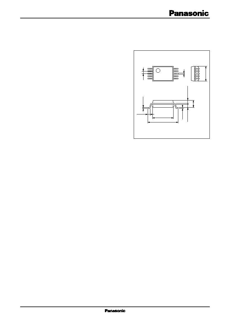
SSOP010-P-0225
Unit: mm
4.3
±
0.30
6.3
±
0.30
0.5
±
0.2
0.1
±
0.1
1
5
10
6
0.2
±
0.1
0.5
3.0
±
0.30
1.5
±
0.2
0.625
±
0.10
0.625
±
0.10
0.15
+0.1
≠0.05
AN8016NSH
Voltage Regulators
3
s
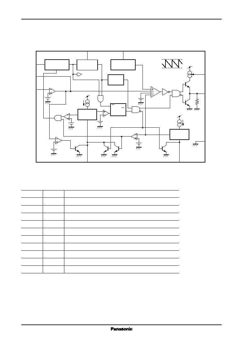
Pin Descriptions
Pin No.
Symbol
Description
1
IN
-
Error amplifier inverting input
2
S.C.P.
Time constant capacitor connection for short-circuit protection
3
SS
Soft-start time-constant capacitor connection
4
Off
On/off control
5
V
CC
Supply voltage
6
Out
Push-pull output
7
GND
Ground
8
RB
Output-current setting resistor connection pin
9
OSC
Oscillator circuit timing resistor/capacitor connection pin
10
FB
Error amplifier output
s
Block Diagram
RB
8
Out
6
GND
7
Off
4
FB
10
IN
-
1
V
CC
5
OSC
9
SS
3
S.C.P
.
2
U.V.L.O.
Error amp.
S.C.P.
comp.
Low level detector
comp.
High level detector comp.
Unlatch comp.
SS pin
Q
R
S
Triangular wave
generator
Latch
Reference
voltage supply
1.27 V
On/off
control
Active-high
Low level
clamp
30 k
0.23 V
5
µ
A
V
CC
1.27 V
0.6 V
1.27 V
V
CC
Low level
clamp
1
µ
A
V
CC
PWM
0.7 V
0.2 V
1.27 V
0.23 V

Voltage Regulators
AN8016NSH
3
Note) 1. Currents or voltages may not be applied to any pins not stipulated above. For circuit currents, a positive (
+
) value indicates
current flowing into the IC, and a negative (
-
) value indicates current flowing out of the IC.
2. Items other than the storage temperature, operating temperature, and power dissipation are all stipulated at T
a
=
25
∞
C.
3. *: T
a
=
85
∞
C. For the independent IC without a heat sink. Note that the relationship between IC power dissipation and
the ambient temperature must follow the derating curve.
s
Absolute Maximum Ratings
Parameter
Symbol
Rating
Unit
Supply voltage
V
CC
15
V
Off pin allowable application voltage
V
OFF
15
V
IN
-
pin allowable application voltage
V
IN
-
V
CC
V
Out pin allowable application voltage
V
OUT
15
V
Supply current
I
CC
mA
Output source current
I
SO(OUT)
-
50
mA
Output sink current
I
SI(OUT)
+
50
mA
Power dissipation
*
P
D
115
mW
Operating temperature
T
opr
-
30 to
+
85
∞
C
Storage temperature
T
stg
-
55 to
+
150
∞
C
s
Recommended Operating Range
Parameter
Symbol
Conditions
Unit
Supply voltage
V
CC
1.8 to 14
V
Off control pin voltage
V
OFF
0 to 14
V
Output source current
I
SO(OUT)
-
40 (min.)
mA
Output sink current
I
SI(OUT)
40 (max.)
mA
Timing resistance
R
T
3 to 30
k
Timing capacitance
C
T
100 to 10 000
pF
Oscillator frequency
f
OUT
20 to 1 000
kHz
Short-circuit protection time
C
SCP
1 000 (min.)
pF
constant setting capacitance
Output current setting resistance
R
B
0 to 10k

AN8016NSH
Voltage Regulators
5
s
Electrical Characteristics at V
CC
=
2.4 V, T
a
=
25
∞
C
Parameter
Symbol
Conditions
Min
Typ
Max
Unit
U.V.L.O. block
Circuit operation start voltage
V
UON
1.45
1.6
1.75
V
Error amplifier block
Input threshold voltage
V
TH
Voltage follower
1.23
1.27
1.31
V
Line regulation with input fluctuation
V
dV
V
CC
=
1.8 V to 14 V
1.0
10
mV
Input bias current
I
B
0.2
1.0
µ
A
High-level output voltage
V
EH
1.85
2.0
2.15
V
Low-level output voltage
V
EL
0.2
V
PWM comparator block
Output source current
I
SS
V
SS
=
0.5 V
-
3.5
-
5
-
6.5
µ
A
Output block
Oscillator frequency
f
OUT
R
T
=
12 k
, C
T
=
330 pF
170
190
210
kHz
Maximum duty
Du
max
75
80
85
%
High-level output voltage
V
OH
I
O
=
-
15 mA, R
B
=
390
1.4
V
Low-level output voltage
V
OL
I
O
=
10 mA, R
B
=
390
0.2
V
Output source current
I
SO(OUT)
V
O
=
0.9 V, R
B
=
390
-
45
-
32
-
20
mA
Output sink current
I
SI(OUT)
V
O
=
0.3 V, R
B
=
390
20
mA
Pull-down resistor
R
O
20
30
40
k
Unlatch circuit block
Input threshold voltage
V
THUL
0.13
0.20
0.27
V
Short-circuit protection circuit block
Input threshold voltage
V
THPC
1.17
1.27
1.37
V
Input standby voltage
V
STBY
60
120
mV
Input latch voltage
V
IN
40
120
mV
Charge current
I
CHG
V
SCP
=
0.5 V
-
1.65
-
1.3
-
0.95
µ
A
On/off control block
Input threshold voltage
V
ON(TH)
0.8
1.0
1.3
V
Off mode SS pin voltage
V
OFF(SS)
0.13
0.27
V
Off mode S.C.P. pin voltage
V
OFF(SCP)
0.13
0.27
V
Whole device
Average consumption current
I
CC(AV)
R
B
=
390
, Duty
=
50%
3.4
5.0
mA
Latch mode consumption current I
CC(LA)
R
B
=
390
1.8
2.4
mA
Standby mode current
I
CC(SB)
5
µ
A
Voltage Regulators
AN8016NSH
5
s
Electrical Characteristics at V
CC
=
2.4 V, T
a
=
25
∞
C (continued)
∑
Design reference data
Note) The characteristics listed below are theoretical values based on the IC design and are not guaranteed.
Parameter
Symbol
Conditions
Min
Typ
Max
Unit
U.V.L.O. block
Reset voltage
V
R
0.8
V
Error amplifier block
V
TH
temperature characteristics
V
THdT
T
a
=
-
30
∞
C to
+
85
∞
C
-
0.5
+
0.5
%
Output source current
I
SO(FB)
V
FB
=
0.5 V
-
40
µ
A
Output sink current
I
SI(FB)
V
FB
=
0.5 V
2
mA
Open-loop gain
A
V
80
dB
PWM comparator block
SS pin voltage
V
SS
1.22
V
Output block
RB pin voltage
V
B
R
B
=
390
0.13
V
Oscillator frequency supply
f
dV
V
CC
=
1.8 V to 14 V
-
1
+
1
%
voltage characteristics
Oscillator frequency temperature
f
dT
T
a
=
-
30
∞
C to 85
∞
C
-
3
+
3
%
characteristics
Short-circuit protection circuit block
Comparator threshold voltage
V
THL
1.27
V
On/off control block
On/Off pin current
I
OFF
V
OFF
=
1.5 V
23
µ
A