 | –≠–ª–µ–∫—Ç—Ä–æ–Ω–Ω—ã–π –∫–æ–º–ø–æ–Ω–µ–Ω—Ç: AN8083S | –°–∫–∞—á–∞—Ç—å:  PDF PDF  ZIP ZIP |
ICs for CD/CD-ROM Player
s
Overview
The AN8083S is an IC for controlling a DC-DC convert-
er suitable for the switching power supply of various
portable equipments. It can operate with input voltage
1.1V or more.
s
Features
∑
Operatable with low voltage input (PV
CC
>1.1V)
∑
Decreased voltage detection circuit built-in
∑
Short-circuit protection feature built-in
∑
Provided with reset output
∑
Synchronizable with outside clock
∑
Low consumption current in stand-by mode
∑
Output voltage in secondary side
;
4.8V
+
0.3V (Variable
by using external resistance)
AN8083S
Low Voltage Operation IC for DC-DC Converter
0.1
±
0.1
1.5
±
0.2
0.3
0.65
0.15
0.4
1
2
3
4
5
6
7
8
16
15
14
13
12
11
10
9
0.4
±
0.25
1.27
Unit : mm
6.5
±
0.3
4.2
±
0.3
10.1
±
0.3
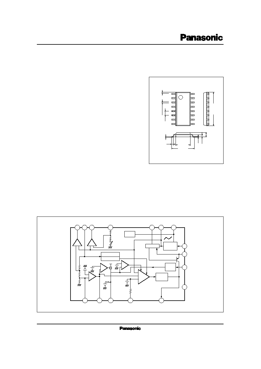
16-lead SOP package (SOP016-P-0225A)
15
13
16
14
7
1
2
3
4
5
6
V
SEN
PV
CC
IN
10
12
9
8
11
Power
OFF
63k
≠
+
GND
0.9V
1.25V
0.7V
4.2V
0.725V
30k
2.0V
4.8V
1.25V
3.0
2.5V
2.15V
0.25V
0.85V
V
REF
≠25
µ
A
≠
+
≠
+
+
≠
+
≠
+
≠
+
RESET
EMP
START
V
REF
CT
CLK
POWER
FB
SPRO
DED
OUT
Starter SW
Early Value Set.
Starter
Switching
Circuit
Triangular
Wave
V
CC
s
Block Diagram

ICs for CD/CD-ROM Player
AN8083S
V
CC
PV
CC
P
D
T
opr
T
stg
Supply Voltage
Power Dissipation
Operating Ambient Temperature
Storage Temperature
V
mW
∞C
∞C
Parameter
Symbol
Rating
Unit
s
Absolute Maximum Ratings
(Ta=25∞C)
14.4
14.4
380
≠20 ~ +75
≠55 ~ +125
Paramenter
Symbol
Range
s
Recommended Operating Range
(Ta=25∞C)
Operating Supply Voltage Range
V
CC
PV
CC
1.8V ~ 12V
1.1V ~ 12V
Parameter
Symbol
Condition
min.
typ.
max.
Unit
s
Electrical Characteristics
(Ta=25∞C)
Power V
CC
Stand-by Mode Supply Current
I
PVCC
2
µ
A
V
CC
=0V, PV
CC
=3V
Power V
CC
Operating Mode Supply Current
I
PVCC
3
mA
1.2
V
CC
=3.1V, PV
CC
=3V
Output Voltage
V
O
V
4.8
Reset Output Threshold Voltage
4
V
TH (RESET)
4.4
V
PV
CC
=3V
Decreased Voltage Detection Threshold Voltage
2.05
V
TH (VSEN)
2.25
V
2.15
PV
CC
=3V
Short-Circuit Protection Operating Voltage
1.35
V
O (SPRO)
2.1
V
V
IN
=0V, V
POWER
=2V
Short-Circuit Protection Operating Voltage
1.7
V
O (SPRO)
3.2
V
V
IN
=1V, V
POWER
=0V
Oscillation Frequency in Normal Operation
60
f
OSC1
80
kHz
70
R
REF
=33k
, CT=330pF
f
OSC2
80
100
120
kHz
Oscillation Frequency at Start
R
REF
=33k
, CT=330pF
V
CC
=1.9V, PV
CC
=3V
Output Voltage (Normal)
1.2
V
OH (OUT)
1.6
V
I
O
= ≠20mA, V
CT
=0V
Output Voltage (Normal)
V
OL (OUT)
0.4
V
I
O
=20mA, V
CT
=1V
Note) Unless otherwise specified, V
CC
=4.8V, PV
CC
=3V
4.2
15
16
13
14
10
7
12
9
8
11
6
5
4
3
2
1
+
2.15V
V
REF
4.8V
4
.
2
V
0
.
7
V
1
.
2
5
V
2.0V
0
.
9
V
30k
≠25
µ
A
63k
+
≠
+
≠
+
≠
+
≠
+
+
≠
3.0V
2.5V
33k
0.01
µ
F
IN
FB
SPRO
47
µ
F
DED
0.01
µ
F
OUT
GND
0.01
µ
F
100
POWER
CLK
PV
CC
4.8V
±
0.3V
33k
330pF
V
REF
CT
START
V
SENSE
EMP
V
CC
+
≠
Power
OFF
0.25V
0.85V
1.25V
*
Connect Pin11 to the secondary side and Pin10 to GND at oscillation start. (Pin10 is always open.)
RESET
0.725V
Starter SW
Initial set
Starter
SW
circuit
+
Triangular
Wave
s
Application Circuit
ICs for CD/CD-ROM Player
AN8083S
s
Pin Description
Pin No.
Symbol
1
IN
∑
Input pin for error amplifier
∑
Threshold voltage ; 0.7V
2
FB
∑
Output pin for error amplifier
∑
Short-circuit protection input pin.
If output of error amplifier does not become "L" when t=CV
th
/I
SPRO
output of IC is not
switched.
I
SPRO
=25
µ
A
V
th
=0.9V
3
SPRO
4
DED
∑
Dead time control input.
Maximum duty ratio set to 85%.
5
OUT
∑
Switching output pin
Output current ; I
O
=20mA (max.)
6
GND
∑
GND pin
∑
Triangular oscillating capacitor pin
7
CT
8
PV
CC
∑
DC voltage input pin
Operates with 1.2V or more.
∑
Clock input
∑ It is used to synchronize triangular oscillation with clock input and operates at rise edge of
clock.
∑ The threshold level is TTL level.
∑ It is open when not used.
9
CLK
∑
Start pin
∑ Starts switching of starter
∑ Threshold voltage, PV
CC
≠ 0.9V
10
START
11
POWER
∑
Power ON/OFF pin
Output ON/OFF switching pin (Output is off at "L.")
Maximum duty ratio can be changed by installing
external resistance between Pins 12 and 4.
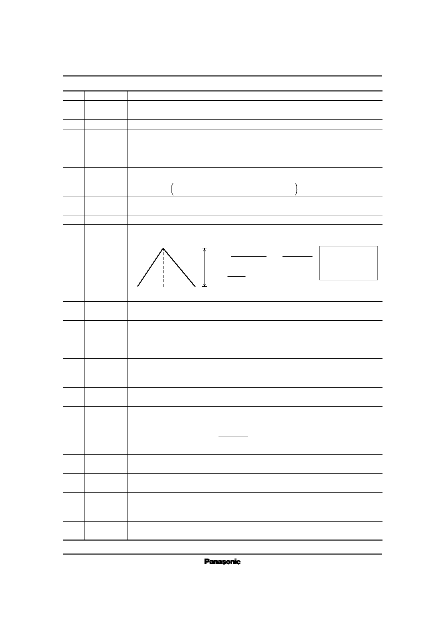
T
1
T
2
V
T
1
=
CV
I (Discharged)
f =
1
T
1
+T
2
T
2
=
CV
I (Charged)
I Discharged=52
µ
A
I Charged=30
µ
A
V=0.58V
∑
Reference voltage pin
∑ 1.25V output
∑ Charged and discharged current of triangular oscillation is determined by external R.
I (Charged) =
V
REF
≠ 0.7
R
REF
+1k
I (Discharged) =1.40
◊
I (Charged)
12
V
REF
13
EMP
∑
Decreased voltage detection output pin
"H" when detected by open collector output form
14
V
SEN
∑
Decreased voltage detection input pin
∑ Threshold voltage ; 2.15V
∑
Reset output pin
∑ "H" when V
CC
becomes 4.2V or more
∑ Open collector output form
15
Reset
16
V
CC
∑
DC voltage input pin
Operates with 1.8V or more.
In normal mode
Pin Description
ICs for CD/CD-ROM Player
AN8083S
8
9
10
11
5
16
13
15
+
1.5V
1.5V
SW
Oscillation starts at "L."
"L" when the battery voltage is 2.15V or less.
"H" when the secondary voltage is 4.2V or more.
Oscillation synchronization signal
Power OFF at "L"
P≠V
CC
V
CC
OUT
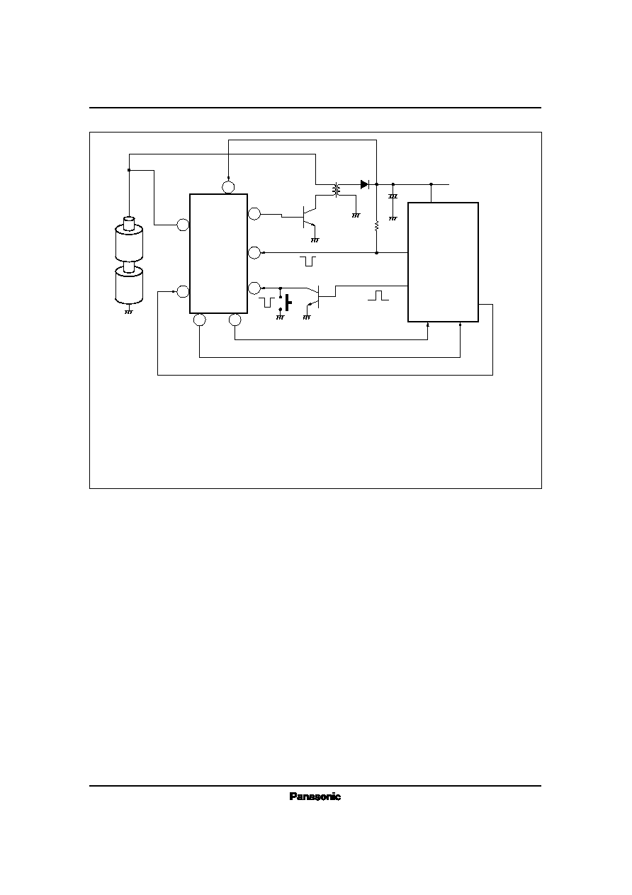
AN8083S
Power SW
Start
CPU
1) When Pin10 becomes "L" by operation of CPU or
push switch, oscillation starts and boosted voltage is
outputted to the secondary side.
2) When the secondary side voltage exceeds 3.6V, starter
circuit is stopped and PWM operation is started by using
the voltage in the secondary side as power supply.
3) When the secondary side voltage becomes 4.2V,
Pin15 becomes "H" and CPU operation is started.
4) When "L" pulse is sent from CPU to Pin11, oscillation
is stopped and it enters the stand-by mode. In this
status consumption current is 2
µ
A max.
5) For re-start, when Pin10 becomes "L" by operation of
CPU or push switch, oscillation starts.
CLK
RESET
EMP
s
Supplementary Explanation
∑ Operational Description
When power V
CC
pin (Pin8) is connected to the supply output and start pin (Pin10) is set to "Low," the triangular oscillation is
outputted to CT pin (Pin7) and the rectangular wave to OUT pin (Pin5). In this condition, called start condition, PWM control is not
obtained and only oscillation is repeated. By this oscillation at start, supply output is increased. This supply output voltage is
inputted to V
CC
pin (Pin16) of the AN8083S. When the voltage of V
CC
pin becomes 3V or more, start oscillation is stopped and
oscillation in normal operation is outputted. PWM control is started only after entering normal mode. The voltage switching
between start and normal operation has 0.5V hysteresis. When power pin (Pin11) is set to "High" in normal operation, normal mode
oscillation is started. In this status, output of the supply is 4.8V fixed.
∑ Other features
1. Short-circuit protection feature
For normal mode oscillation, when output/FB pin (Pin2) of error amplifier is in "High" condition, oscillation is stopped, since the
power supply system is judged to be in an abnormal condition. With the time constant of discharged current I
SPRO
of SPRO pin
(Pin3) and capacitor C
SPRO
, pin voltage is increased, and oscillation is stopped when it becomes 1.25V or more. During this time,
when the error amplifier becomes "Low," charged current no longer exits and SPRO is maintained to 0.9V.
2. Decreased voltage detection circuit
When V
SEN
pin (Pin14) gets 2.15V or less, EMS pin (Pin13) gets "High."
3. Reset output
When V
CC
pin voltage is 4.2V or more, RST pin (Pin15) gets "High."
s
System Block Diagram
ICs for CD/CD-ROM Player
AN8083S
∑
Miscellaneous
1. Method for making output voltage variable
V
CC
= 0.7V
◊
(R
1
+ R
2
)/R
2
R
1
= R
X
// R
3
R
2
= R
Y
// R
4
ex) Where V
CC
= 5V,
R
X
= 51k
R
Y
= 7.5k
2. Method for making decreased voltage detection variable
V
SEN
=
R
1
+ R
2
◊
1.25
R
2
ex) V
SEN
= 3V
V
SEN
=
R
1
+ R
2
+ R
3
◊
1.25
R
2
R
3
= 7k
However, take care that an external resistance causes different temperature characteristics.
3. Reset output
When the output voltage is made variable, detection voltage changes.
V
CC
= 4.8V
4.2V (No changes)
V
CC
= 5V
4.27V
∑
Chopper type application
51k
7.5k
3.64k
3.5k
15
1.25V
1
6
.
8
6
k
16
1
51k
16
1
2
8
5
AN8083S
33k
0.01
µ
F
100
0.01
µ
F
100
0.01
µ
F
2SD1328
2SD1328
4.8V
±
0.3V
R
X
R
Y
R
3
=20.5k
R
4
=3.5k
V
CC
(16)
IN (1)
R
1
=7k
R
2
=10k
V
SEN
(14)
R
3
7.5k