Voltage Regulators
1
Publication date: November 2001
SFF00009CEB
AN80MxxRSP Series
5-pin, low dropout voltage regulator with standby function (500 mA type)
I Overview
The AN80MxxRSP series is a 0.5 A, low dropout
voltage regulator IC with standby function, featuring low
current consumption and low noise.
I Features
∑ Standby consumption current: max. 3 µA
∑ Dropout voltage: 0.25 V
∑ Output voltage accuracy: ±3%
∑ 5-pin surface mounting package
∑ Ripple rejection ratio: 30 dB (f = 500 kHz)
∑ Output voltage: 1.8 V, 1.9 V, 2.0 V, 2.1 V, 2.2 V, 2.5 V,
2.7 V, 2.8 V, 2.9 V, 3.0 V, 3.1 V, 3.2 V,
3.3 V, 3.4 V, 3.5 V, 3.6 V, 4.8 V, 4.9 V,
5.0 V, 5.1 V, 5.2 V, 5.3 V
I Applications
∑ General use power supply
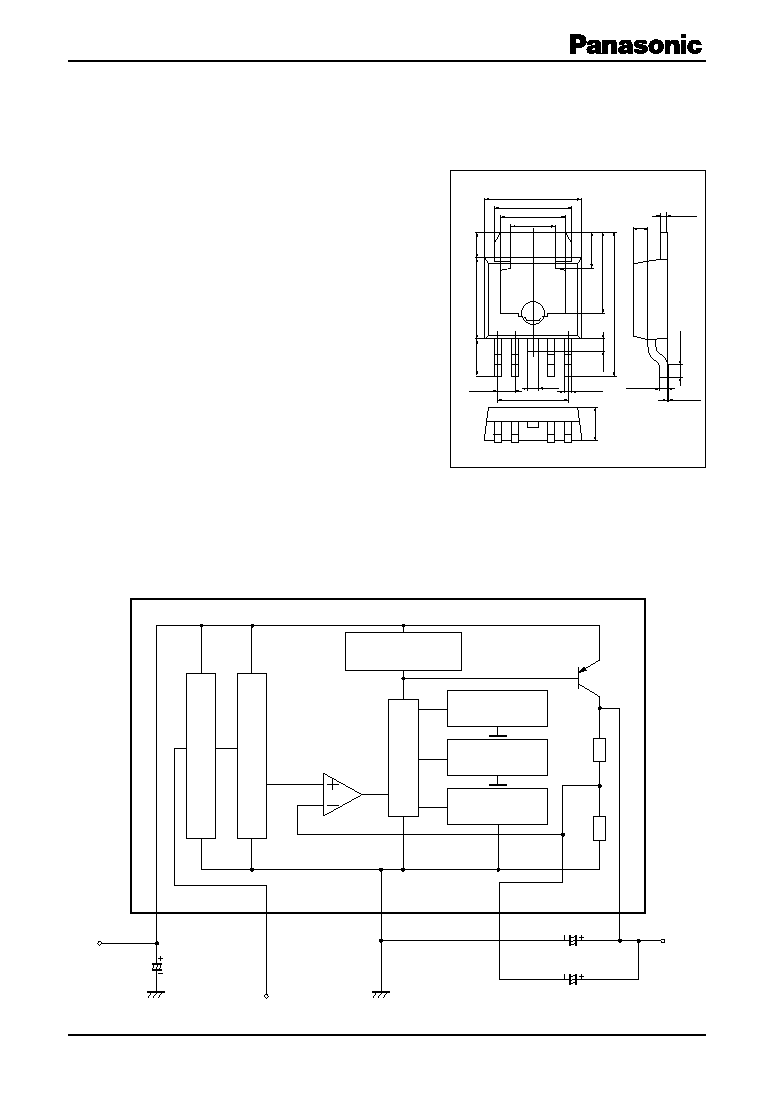
I Block Diagram
Unit: mm
SP-5SU
(3.00)
(4.35)
5.40
±0.10
6.50
±0.10
1.80
±
0.10
(0.80)
(2.50)
2.30
±
0.10
(5.50)
9.80
±
0.20
5.08
±0.10
1
2
4
5
0.50
±0.10
0.50
±0.10
0.10
±0.10
1.00
±
0.20
1.00
±0.10
5.50
±
0.10
(2.50)
1.27
±0.10
3
(0.75)
0.50
±0.10
V
IN
V
OUT
Cont.
C
IN
(Fin)
3.3
µF
C
OUT
33
µF
C
NR
1
µF
1
2
3
4
5
Input short-circuit
protection
Output stage
Overcurrent
limitter
Starter
V
oltage reference
Error amplifier
Thermal
protection
Inrush current
protection
V
REF
R1
R2
Output dri
v
e
r
Note) The package of this product will be changed
to lead-free type (SP-5SUA). See the new pack-
age dimensions section later of this datasheet.
AN80MxxRSP Series
2
SFF00009CEB
I Pin Descriptions
Pin No.
Description
1
Input voltage pin (V
IN
)
2
Control pin (Cont.) High: operation, Low: stop
3
Grounding pin (GND) Electrically in common with radiation fin
4
Noise reduction pin (N.R.) Open when the noise reduction function is not used
5
Output voltage pin (V
OUT
)
I Absolute Maximum Ratings
Parameter
Symbol
Rating
Unit
Supply voltage
V
CC
14.4
V
Supply current
I
CC
mA
Power dissipation
*1
P
D
255
mW
Operating ambient temperature
*2
T
opr
-30 to +85
∞C
Storage temperature
*2
T
stg
-55 to +150
∞C
Note) 1. The output voltage may exceed the rated value if T
j
> 150∞C in no-load condition. Set to I
O
> 5 mA if T
j
is likely to exceed
150
∞C.
2. This IC is not suitable for automobile equipment use.
3. *1: The above power dissipation shows the value of an independent IC without heat sink at T
a
= 85∞C. For details, refer to
"2. Power dissipation of SP-5SU package" in the Application Notes.
*2: Except for the operating ambient temperature and storage temperature, all ratings are for T
a
= 25∞C.
AN80MxxRSP Series
3
SFF00009CEB
I Recommended Operating Conditions
Part No.
Output voltage
Operating supply voltage range (V
CC
)
Unit
AN80M18RSP
1.8
2.3 to 14.0
V
AN80M19RSP
1.9
2.4 to 14.0
V
AN80M20RSP
2.0
2.5 to 14.0
V
AN80M21RSP
2.1
2.6 to 14.0
V
AN80M22RSP
2.2
2.7 to 14.0
V
AN80M25RSP
2.5
3.0 to 14.0
V
AN80M27RSP
2.7
3.2 to 14.0
V
AN80M28RSP
2.8
3.3 to 14.0
V
AN80M29RSP
2.9
3.4 to 14.0
V
AN80M30RSP
3.0
3.5 to 14.0
V
AN80M31RSP
3.1
3.6 to 14.0
V
AN80M32RSP
3.2
3.7 to 14.0
V
AN80M33RSP
3.3
3.8 to 14.0
V
AN80M34RSP
3.4
3.9 to 14.0
V
AN80M35RSP
3.5
4.0 to 14.0
V
AN80M36RSP
3.6
4.1 to 14.0
V
AN80M48RSP
4.8
5.3 to 14.0
V
AN80M49RSP
4.9
5.4 to 14.0
V
AN80M50RSP
5.0
5.5 to 14.0
V
AN80M51RSP
5.1
5.6 to 14.0
V
AN80M52RSP
5.2
5.7 to 14.0
V
AN80M53RSP
5.3
5.8 to 14.0
V
AN80MxxRSP Series
4
SFF00009CEB
Parameter
Symbol
Conditions
Min
Typ
Max
Unit
Output voltage
V
OUT
V
IN
= 2.8 V, I
OUT
= 250 mA
1.746
1.8
1.854
V
Line regulation
REG
IN
V
IN
= 2.8 V 14.0 V, I
OUT
= 250 mA
18
mV
Load regulation
REG
LOA
V
IN
= 2.8 V, I
OUT
= 0 mA 500 mA
36
mV
Peak output current
I
PEAK
V
IN
= 2.8 V, The output current value 600
900
mA
when V
OUT
decreases by 5% from
its value at I
OUT
= 250 mA.
Bias current under no load
I
BIAS
V
IN
= 2.8 V, I
OUT
= 0 mA
1.1
3.0
mA
Bias current fluctuation to input
I
BIAS(IN)
V
IN
= 2.8 V 14.0 V, I
OUT
= 250 mA
-5
5
mA
Bias current fluctuation to load
I
BIAS(LOA)
V
IN
= 2.8 V, I
OUT
= 0 mA 500 mA
25
mA
Standby consumption current
I
STB
V
IN
= 14.0 V, V
CONT
= 0 V
3.0
µA
Bias current before starting regulation
I
RUSH
V
IN
= 1.71 V, I
OUT
= 0 A
5
mA
Control terminal current
I
CONT
V
IN
= 2.8 V, I
OUT
= 250 mA
30
µA
V
CONT
= 1.8 V
Ripple rejection ratio 1
RR1
V
IN
= 3.8 V±1 V, f = 120 Hz
58.8
dB
I
OUT
= 100 mA
Minimum input/
V
DIF(min)1
V
IN
= 1.9 V, I
OUT
= 250 mA
0.25
0.45
V
output voltage difference 1
Minimum input/
V
DIF(min)2
V
IN
= 2.0 V, I
OUT
= 500 mA
0.8
V
output voltage difference 2
Control terminal threshold high voltage
V
CONTH
V
IN
= 2.8 V
1.45
1.80
V
Control terminal threshold low voltage
V
CONTL
V
IN
= 2.8 V
0.50
0.70
V
Parameter
Symbol
Conditions
Min
Typ
Max
Unit
Ripple rejection ratio 2
RR2
V
IN
= 3.8 V±1 V, f = 500 kHz
30
dB
I
OUT
= 100 mA
Output noise voltage
V
NO
10 Hz
f 100 kHz, I
OUT
= 100 mA
40
µV[rms]
V
IN
= 2.8 V, CNR = 1 µF
Output voltage temperature
dV
OUT
V
IN
= 2.8 V, I
OUT
= 5 mA
±40
ppm/∞C
coefficient
dT
a
-30∞C T
a
+125∞C
Output short-circuit current
I
OSHORT
V
IN
= 14.0 V, V
OUT
= GND
300
mA
Overheat protection operating
T
jTH
V
IN
= 2.8 V, I
OUT
= 5 mA
150
∞C
temperature
I Electrical Characteristics at T
a
= 25∞C
∑ AN80M18RSP (1.8 V type)
Unless otherwise specially provided, shorten each test time (within 10 ms) so that the test is conducted under the condition that
the drift due to the temperature increase in the chip junction part can be neglected. C
IN
= 3.3 µF, CNR = Open, C
OUT
= 33 µF
∑ Design reference data
Note) The following values are typical and not guaranteed values.
AN80MxxRSP Series
5
SFF00009CEB
Parameter
Symbol
Conditions
Min
Typ
Max
Unit
Output voltage
V
OUT
V
IN
= 2.9 V, I
OUT
= 250 mA
1.843
1.9
1.957
V
Line regulation
REG
IN
V
IN
= 2.9 V 14.0 V, I
OUT
= 250 mA
19
mV
Load regulation
REG
LOA
V
IN
= 2.9 V, I
OUT
= 0 mA 500 mA
38
mV
Peak output current
I
PEAK
V
IN
= 2.9 V, The output current value 600
900
mA
when V
OUT
decreases by 5% from
its value at I
OUT
= 250 mA.
Bias current under no load
I
BIAS
V
IN
= 2.9 V, I
OUT
= 0 mA
1.1
3.0
mA
Bias current fluctuation to input
I
BIAS(IN)
V
IN
= 2.9 V 14.0 V, I
OUT
= 250 mA
-5
5
mA
Bias current fluctuation to load
I
BIAS(LOA)
V
IN
= 2.9 V, I
OUT
= 0 mA 500 mA
25
mA
Standby consumption current
I
STB
V
IN
= 14.0 V, V
CONT
= 0 V
3.0
µA
Bias current before starting regulation
I
RUSH
V
IN
= 1.805 V, I
OUT
= 0 A
5
mA
Control terminal current
I
CONT
V
IN
= 2.9 V, I
OUT
= 250 mA
30
µA
V
CONT
= 1.8 V
Ripple rejection ratio 1
RR1
V
IN
= 3.9 V±1 V, f = 120 Hz
58.4
dB
I
OUT
= 100 mA
Minimum input/
V
DIF(min)1
V
IN
= 2.0 V, I
OUT
= 250 mA
0.25
0.45
V
output voltage difference 1
Minimum input/
V
DIF(min)2
V
IN
= 2.1 V, I
OUT
= 500 mA
0.8
V
output voltage difference 2
Control terminal threshold high voltage
V
CONTH
V
IN
= 2.9 V
1.45
1.80
V
Control terminal threshold low voltage
V
CONTL
V
IN
= 2.9 V
0.50
0.70
V
Parameter
Symbol
Conditions
Min
Typ
Max
Unit
Ripple rejection ratio 2
RR2
V
IN
= 3.9 V±1 V, f = 500 kHz
30
dB
I
OUT
= 100 mA
Output noise voltage
V
NO
10 Hz
f 100 kHz, I
OUT
= 100 mA
40
µV[rms]
V
IN
= 2.9 V, CNR = 1 µF
Output voltage temperature
dV
OUT
V
IN
= 2.9 V, I
OUT
= 5 mA
±40
ppm/∞C
coefficient
dT
a
-30∞C T
a
+125∞C
Output short-circuit current
I
OSHORT
V
IN
= 14.0 V, V
OUT
= GND
300
mA
Overheat protection operating
T
jTH
V
IN
= 2.9 V, I
OUT
= 5 mA
150
∞C
temperature
I Electrical Characteristics at T
a
= 25∞C (continued)
∑ AN80M19RSP (1.9 V type)
Unless otherwise specially provided, shorten each test time (within 10 ms) so that the test is conducted under the condition that
the drift due to the temperature increase in the chip junction part can be neglected. C
IN
= 3.3 µF, CNR = Open, C
OUT
= 33 µF
∑ Design reference data
Note) The following values are typical and not guaranteed values.