 | –≠–ª–µ–∫—Ç—Ä–æ–Ω–Ω—ã–π –∫–æ–º–ø–æ–Ω–µ–Ω—Ç: AN8377N | –°–∫–∞—á–∞—Ç—å:  PDF PDF  ZIP ZIP |
ICs for CD/CD-ROM Player
s
Overview
The AN8377N is an IC which incorporates 3 circuits of
BTL drivers for driving various DC motors such as actua-
tors (focus, tracking, traverse), spindles, and loading of
the CD players, and the +5V low drop type power supply.
s
Features
∑
Operating supply voltage range ; V
CC
=5.5V to 18V
∑
Built-in 3 circuits of voltage BTL drivers
(maximum drive current : 500mA)
∑
Stable circuit operation against supply voltage change
and temperature change due to the built-in stabilized
power supply
∑
Built-in +5V low drop power supply (external PNP
power transistor)
∑
Built-in reset circuit (reset voltage : 4.82V)
∑
Built-in thermal protective circuit (operating tempera-
ture : 159 ; typ.)
∑
Built-in power cut circuit (motor driver 1 only)
s
Applications
Linear driving of the DC motors and actuators of the
CD players, CD radio cassette tape recorder, and so on.
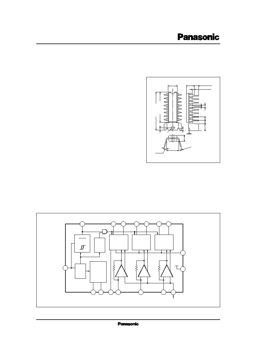
AN8377N
3-channel Linear Driver
1
2
3
4
5
6
7
8
10
9
11
12
13
14
15
16
27.4
±
0.3
6.35
±
0.3
4.70.25
3.05
±
0.25
0.5
±
0.1
1.2
±
0.25
2.54
1.5
±
0.1
3.80
±
0.3
17
7.62
±
0.25
0 ~ 6∞
0.45
+ 0.1
≠ 0.05
0.560.1
¯2.1
Unit : mm
1.7
2.54
1.06
±
0.25
21.6
±
0.3
5.08
±
0.1
16-Lead DIP Package with Fin (HDIP016-P-0300)
15
13
14
9
10
11
12
1
F
2
3
4
16
5
7
6
8
+
≠
Error
Amp.
100kW
+
≠
Error
Amp.
100kW
+
≠
Error
Amp.
100kW
RST
Thermal
Shutdown
BTL
Motor
Driver 1
BTL
Motor
Driver 3
BTL
Motor
Driver 2
Band≠
gap
(2.5V)
5V
Regulator
(low≠sat)
P V
CC
GND
V
CC
V
REF
(
1
/
2
V
CC
)
s
Block Diagram

ICs for CD/CD-ROM Player
AN8377N
s
Absolute Maximum Ratings
(Ta=25∞C)
V
CC
P
D
T
opr
T
stg
Supply Voltage
Power Dissipation
Operating Ambient Temperature
Storage Temperature
V
mW
∞C
∞C
Parameter
Symbol
Rating
Unit
20
1500
≠25 ~ +80
≠55 ~ +150
s
Recommended Operating Range
(Ta=25∞C)
Parameter
Symbol
Range
Operating Supply Voltage Range
V
CC
5.5V ~ 16V
s
Electrical Characteristics
(Ta=25∞C)
V
CC
=12V
V
CC
=12V, R
L
=50W
V
CC
=12V, R
L
=50W ~ 25W
V
CC
=15.5V ~ 5.5V , R
L
=50W
Parameter
Symbol
Condition
min.
typ.
max.
Unit
10.5
5
4.82
No Load Current
5V Regulator Output Voltage
5V Regulator Load Change
5V Regulator Input Change
Reset Threshold Voltage
I
CC
V
RO
DV
RI
DV
RVC
V
RST
mA
V
mV
mV
V
7
4.75
≠15
≠15
4.55
15
5.25
30
50
5.1
Note) The specified values of V
IOF
, V
OOF
, G
+
, G
R
, V
L+
, V
L≠
, and V
DZ
are common ones for each of the motor driver 1, motor driver 2,
and motor driver 3 circuits.
Reset Threshold Hysteresis Width
Motor Driver 2 Output Voltage at Reset
Motor Driver 3 Output Voltage at Reset
Motor Driver 1 Output Voltage at Reset
5V Regulator External Transistor Base
Current Limit Value
Minimum V
CC
Voltage
at which V15=Low
Reset Operating Minimum Voltage
Input Offset Voltage
Output Offset Voltage
Gain (+)
(+) (≠) Relative Gain
Limit Voltage (+)
Limit Voltage (≠)
Dead Zone Width
PC Input Threshold (L)
PC Input Threshold (H)
Thermal Protective Circuit Operating
Temperature Balancing Value
Thermal Protective Circuit Operating
Temperature Hysteresis Width
V
HYS
V
R (min.)
V
IOF
V
OOF
G
+
G
R
V
L+
V
L≠
V
DZ
V
PCL
V
PCH
V
2RS
V
3RS
V
1RS
I
3LIM
T
THD
DT
THD
V
CC
=18V, R
L
=20W,
R
IN
=10kW
V
CC
=18V, R
L
=20W,
R
IN
=10kW
V
CC
=18V, R
L
=20W,
R
IN
=10kW
V
CC
=18V, R
L
=20W,
R
IN
=10kW
V
CC
=18V, R
L
=20W,
R
IN
=10kW
V
CC
=18V, R
L
=20W,
R
IN
=10kW
V
CC
=18V, R
L
=20W,
R
IN
=10kW
V
CC
=18V
V
CC
=18V
V
CC
=3.5V, R
L
=10kW
V
CC
=3.5V, R
L
=10kW
V
CC
=3.5V, R
L
=10kW
90
3.1
≠7
≠50
16.5
≠ 0.85
7.1
≠10.9
≠10
2.8
≠50
≠50
≠50
9
170
20
12
159
64
310
7
50
22.5
0.85
10.9
≠7.1
30
1.2
50
50
50
16
mV
V
mV
mV
dB
dB
V
V
mV
V
V
mV
mV
mV
mA
∞C
∞C
ICs for CD/CD-ROM Player
AN8377N
(Used when driving the focus, tracking actuator, and traverse motor)
1
3
4
5
6
7
8
16
14
13
12
11
10
9
M
+
AN8377N
15
20kW
+5V
from
MN6622
or
MN6625
PV
CC
2
V
CC
(shot circuit possible)
A1547
5V
22 F
m
M
o
t
o
r
D
r
i
v
e
r
1
M
o
t
o
r
D
r
i
v
e
r
2
M
o
t
o
r
D
r
i
v
e
r
3
V
REF
(typ.2.5V)
F
s
Pin Descriptions
(The following description applies when the 3 channels for the motor drivers 1, 2, and 3 are used.)
Description
I/O
Pin No.
Equivalent Circuit
DC Voltage
(V
CC
/12V)
Symbol
1
PV
CC
I
12V
Power V
CC
pin.
Supplies a current flowing to
the output power transistor.
2
V
CC
I
12V
V
CC
pin.
Not connected to the power
V
CC
pin.
3
TB
O
11.3V
External PNP transistor base
connection pin
4
V
MON
I
5V
External
PNP
transistor
collector connection pin
(=5V output pin)
33
10kW
10kW
1
2
3
4
s
Application Circuit

ICs for CD/CD-ROM Player
AN8377N
s
Pin Descriptions (Cont.)
(The following description applies when the 3 channels for the motor drivers 1, 2, and 3 are used.)
Description
I/O
Pin No.
Equivalent Circuit
DC Voltage
(V
CC
/12V)
Symbol
15
RST
O
Reset output pin.
Open collector output type.
F
GND
I
0V
GND pin
8
V
REF
I
2.5V
V
REF
input pin
5
TVDI
I
2.5V
6
FDI
I
2.5V
7
TDI
I
2.5V
9
TD ≠
O
(0.3V)
10
TD+
O
(0.3V)
11
FD ≠
O
(0.3V)
12
FD+
O
(0.3V)
13
TVD ≠
O
(0V)
14
TVD+
O
(0V)
Driver 1 error input pin
Driver 2 error input pin
Driver 3 error input pin
BTL driver 3 inverting output
pin
BTL driver 3 non-inverting
output pin
BTL driver 2 inverting output
pin
BTL driver 2 non-inverting
output pin
BTL driver 1 inverting output
pin
BTL driver 1 non-inverting
output pin
16
PC
I
0V
PC (power cut) input pin
200W
500W
or
or
(P V
CC
)
∑ ∑ ∑ ∑
15
F
8
5
6
or
7
9
or
11
13
or
10
or
12
14
16