 | –≠–ª–µ–∫—Ç—Ä–æ–Ω–Ω—ã–π –∫–æ–º–ø–æ–Ω–µ–Ω—Ç: AN8480NSB | –°–∫–∞—á–∞—Ç—å:  PDF PDF  ZIP ZIP |
ICs for Compact Disc/CD-ROM Player
1
AN8480NSB
3-phase full-wave motor driver IC
s
Overview
The AN8480NSB is a 3-phase full-wave motor
driver IC with a reverse rotation brake/short brake
changeover function, incorporating a thermal pro-
tection circuit with its protection monitor pin.
s
Features
∑
3-phase full-wave and snubberless
∑
FG output
∑
Current limit
∑
Reverse rotation prevention
∑
Thermal protection circuit built-in (with thermal
protection monitor pin)
s
Applications
∑
Various types of optical disk drive
s
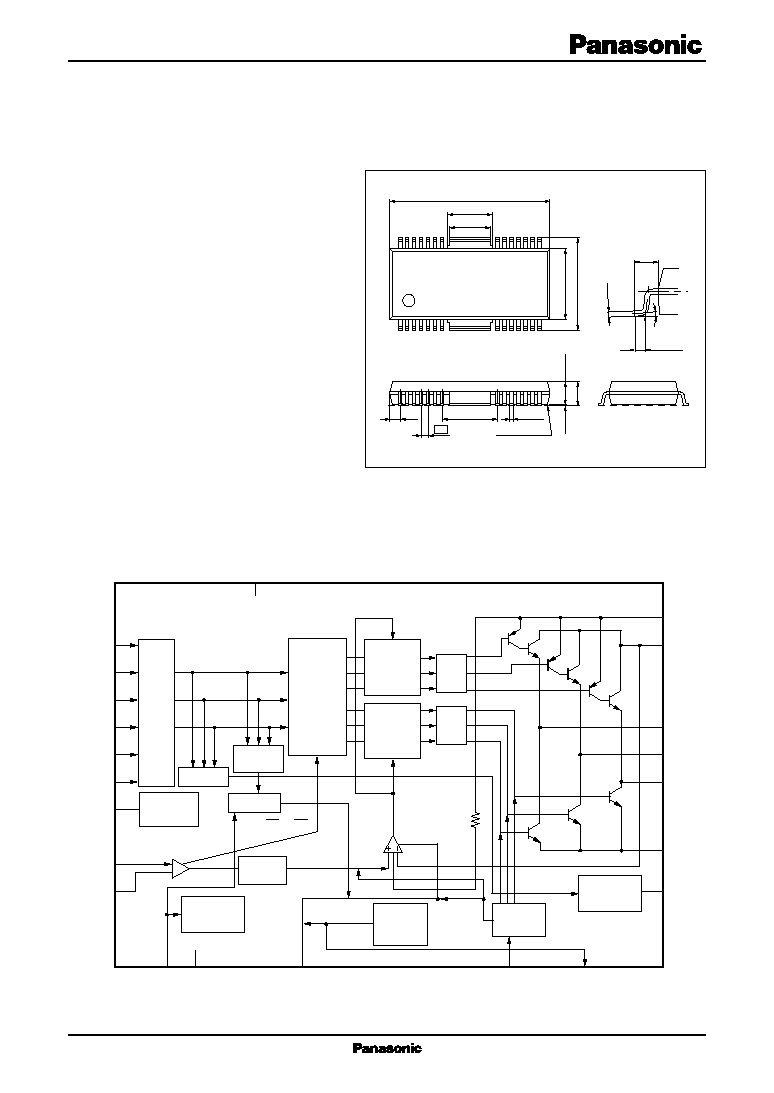
Block Diagram
Unit: mm
HSOP042-P-0400
1
7
8
14
(1.315)
0.65±0.20
28
22
21
(4.8)
(6.4)
(1.2)
(5.15)
18.4±0.2
8.3±0.2
2.7±0.2
0.1±0.1
10.93±0.30
15
0.35
+0.10
≠0.05
0.30
+0.10
≠0.05
0.8
Seating plane
0
∞
to 10
∞
15
13
11
20
16
10
17
18
12
1
26
27
28
22
21
7
9
8
6
5
2
3
Hall
bias
Start/stop
Thermal
protection
circuit
Absolute
value
Brake
circuit
Hall
amp.
matrix
Detection
Upper side
distribution
Lower side
distribution
Logic
Amp.
Amp.
Direction
detection
Direction
changeover
EA
ER
VTL
S/S
V
CC
PCI
BRK
TSDF
ECR
EC
VH
H3
-
H3
+
H2
-
H2
+
H1
-
H1
+
SG
EP
=
ER
◊
FG
comparator
VM
CS1
A1
A2
A3
PG
FG

AN8480NSB
ICs for Compact Disc/CD-ROM Player
2
s
Pin Descriptions
s
Absolute Maximum Ratings
Parameter
Symbol
Rating
Unit
Supply voltage
V
CC
7.0
V
V
M
14.4
Control signal input voltage
*4
V
(n)
0 to V
CC
V
Supply current
I
CC
30
mA
Output current
*3
I
O(n)
±
1 200
mA
Hall bias current
I
HB
50
mA
Power dissipation
*2
P
D
667
mW
Operating ambient temperature
*1
T
opr
-
20 to
+
70
∞
C
Storage temperature
*1
T
stg
-
55 to
+
150
∞
C
Note) Do not apply external currents or voltages to any pins not specifically mentioned.
For circuit currents, '
+
' denotes current flowing into the IC, and '
-
' denotes current flowing out of the IC.
*1: Except for the operating ambient temperature and storage temperature, all ratings are for T
a
=
25
∞
C.
*2: For 70
∞
C and IC alone.
*3: n
=
1, 22, 26, 27, 28
*4: n
=
2, 3, 5, 6, 8, 9, 10, 13, 17, 18
Pin No. Symbol
Description
15
SG
Signal GND pin
16
V
CC
Supply voltage pin
17
ECR
Torque command reference input pin
18
EC
Torque command input pin
19
N.C.
N.C.
20
PCI
Current feedback phase compensation pin
21
VM
Motor supply voltage pin
22
CS
Current det. pin 1
23
N.C.
N.C.
24
N.C.
N.C.
25
N.C.
N.C.
26
A3
Drive output 3
27
A2
Drive output 2
28
A1
Drive output 1
Pin No. Symbol
Description
1
PG
Power GND pin
2
H1
+
Hall element-1 positive input pin
3
H1
-
Hall element-1 negative input pin
4
N.C.
N.C.
5
H2
+
Hall element-2 positive input pin
6
H2
-
Hall element-2 negative input pin
7
VH
Hall bias pin
8
H3
+
Hall element-3 positive input pin
9
H3
-
Hall element-3 negative input pin
10
SS
Start/stop changeover pin
11
TFLG
Thermal protection monitor pin
12
FG
FG signal output pin
13
BRK
Brake mode setting pin
14
N.C.
N.C.
s
Recommended Operating Range
Parameter
Symbol
Range
Unit
Supply voltage
V
CC
4.25 to 5.5
V
V
M
4.5 to 14

ICs for Compact Disc/CD-ROM Player
AN8480NSB
3
s
Electrical Characteristics at T
a
=
25
∞
C
Parameter
Symbol
Conditions
Min
Typ
Max
Unit
Overall
Circuit current 1
I
CC1
V
CC
=
5 V in power save mode
0
0.1
mA
Circuit current 2
I
CC2
V
CC
=
5 V, I
O
=
0 mA
1
8
16
mA
Start/stop
Start voltage
V
START
Voltage with which a circuit operates
2.7
V
at V
CC
=
5 V and L
H
Stop voltage
V
STOP
Voltage with which a circuit becomes
0.7
V
off at V
CC
=
5 V and H
L
Medium voltage
V
MED
Voltage with which V
PC1
becomes
1.55
1.75
V
low at V
CC
=
5 V and EC
=
0 V
Hall bias
Hall bias voltage
V
HB
V
CC
=
5 V, I
HB
=
20 mA
0.7
1.2
1.6
V
Hall amplifier
Input bias current
I
BH
V
CC
=
5 V
1
5
µ
A
In-phase input voltage range
V
HBR
V
CC
=
5 V
1.5
4.0
V
Minimum input level
V
INH
V
CC
=
5 V
60
mV[p-p]
Torque command
In-phase input voltage range
EC
V
CC
=
5 V
0.5
3.9
V
Offset voltage
EC
OF
V
CC
=
5 V
-
100
0
100
mV
Dead zone
EC
DZ
V
CC
=
5 V
25
75
125
mV
Input current
EC
IN
V
CC
=
5 V, EC
=
ECR
=
1.65 V
-
5
-
1
µ
A
Input/output gain
A
CS
V
CC
=
5 V, R
CS
=
0.5
0.75
1.0
1.25
A/V
Output
High-level output saturation voltage
V
OH
V
CC
=
5 V, I
O
=
-
300 mA
0.9
1.6
V
Low-level output saturation voltage
V
OL
V
CC
=
5 V, I
O
=
300 mA
0.2
0.6
V
Torque limit current
I
TL
V
CC
=
5 V, R
CS
=
0.5
400
500
600
mA
FG
FG output high-level
FG
H
V
CC
=
5 V, I
FG
=
-
0.01 mA
3.0
V
CC
V
FG output low-level
FG
L
V
CC
=
5 V, I
FG
=
0.01 mA
0.5
V
In-phase input voltage range
V
FGR
V
CC
=
5 V,
1.5
3.0
V
Input D-range at H2
+
, H2
-
FG hysteresis width
H
FG
V
CC
=
5 V
1
10
20
mV
Brake cirrcuit
Short brake model level
V
SBR
V
CC
=
5 V
1.0
V
Reverse rotation brake mode level
V
RBR
V
CC
=
5 V
3.5
V
Short brake start level
V
SBRL
V
CC
=
5 V, ECR
=
1.65 V
1.65
1.74
V
Short brake current
I
SBR
V
CC
=
5 V
12
35
mA
AN8480NSB
ICs for Compact Disc/CD-ROM Player
4
s
Electrical Characteristics at T
a
=
25
∞
C (continued)
∑
Design reference data
Note) The characteristics listed below are theoretical values based on the IC design and are not guaranteed.
Parameter
Symbol
Conditions
Min
Typ
Max
Unit
Thermal protection
Thermal protection operating
T
SDON
V
CC
=
5 V,
EC
=
100 mV
160
∞
C
temperature
Thermal protection hysteresis width
T
SD
V
CC
=
5 V,
EC
=
100 mV
45
∞
C
Thermal protection flag
Level at thermal protection
=
on
V
TSDON
V
CC
=
5 V
0.5
V
Level at thermal protection
=
off
V
TSDOFF
V
CC
=
5 V
3.0
V
s
Usage Notes
Prevent this IC from being line-to-ground fault. (To be concrete, do not short-circuit any of A1 (pin 28), A2 (pin 27)
and A3 (pin 26) with VM pin (pin 21).)
s
Application Notes
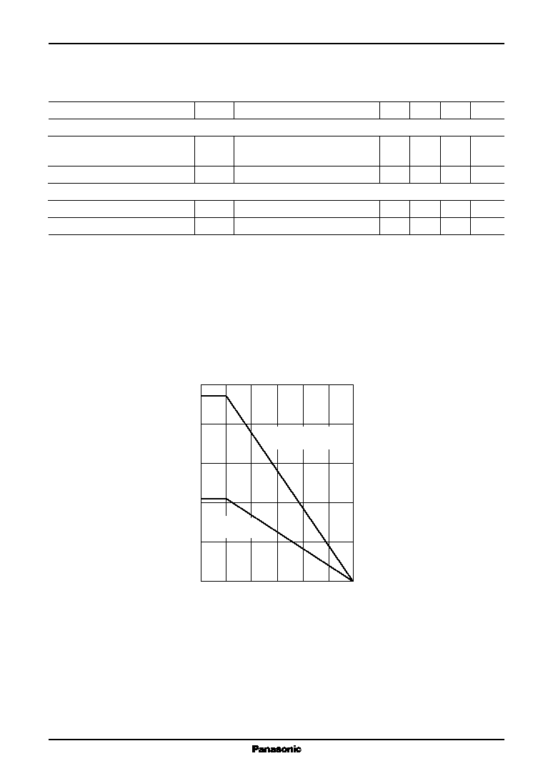
∑
P
D
T
a
curves of HSOP042-P-0400
P
D
T
a
0.000
0.500
1.042
1.000
1.500
2.000
2.240
2.500
Mounted on standard board
(glass epoxy: 75
◊
75
◊
t1.6 mm
3
)
R
th(j-a)
=
55.8
∞
C/W
Independent IC
without a heat sink
R
th(j-a)
=
119.9
∞
C/W
Power dissipation
P
D
(W)
0
25
Ambient temperature T
a
(
∞
C)
50
125
75
100
150
ICs for Compact Disc/CD-ROM Player
AN8480NSB
5
s
Application Notes (continued)
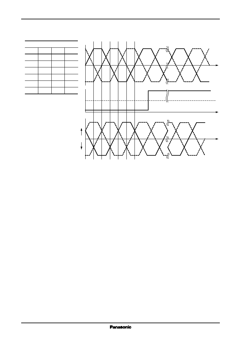
∑
Phase conditions between Hall input and output current
A
B
C
D
E
F
Phase of Hall pin
H1
+
H3
+
H2
+
H
M
L
H
M
L
M
L
H
L
M
H
L
M
H
M
L
H
ECR
EC
A
B
C
D
E
H1
H2
H2
H1
H3
H3
A3
A3
A2
A1
A2
A1
F
0
0
0
Emit
Output current
Sink
∑
Power consumption calculation method
You can find a rough value of electric power to be consumed in the IC in the following method and the use of EXCEL
(computer soft ware) will enable you to put it on a graph.
Calculating formula:
1. Let an induced voltage generated in each phase as below:
(Reference to a motor center point)
E
A1
=
E
O
◊
sin (X) ∑ ∑ ∑ (1)
E
A2
=
E
O
◊
sin (X
+
120) ∑ ∑ ∑ (2)
E
A3
=
E
O
◊
sin (X
+
240) ∑ ∑ ∑ (3)
X: Phase angle
2. Let a current flowing in each phase as below:
I
A1
=
I
O
◊
sin (X) ∑ ∑ ∑ (4)
I
A2
=
I
O
◊
sin (X
+
120) ∑ ∑ ∑ (5)
I
A3
=
I
O
◊
sin (X
+
240) ∑ ∑ ∑ (6)
3. The voltages generated by a wire-wound resistance of a motor are:
V
R1
=
I
A1
◊
R ∑ ∑ ∑ (7)
V
R2
=
I
A2
◊
R ∑ ∑ ∑ (8)
V
R3
=
I
A3
◊
R ∑ ∑ ∑ (9)
4. In each phase, add the voltage generated by an induced voltage and that by a wire-wound resistance.
V
A1
'
=
(1)
+
(4)
V
A2
'
=
(2)
+
(5)
V
A3
'
=
(3)
+
(6)
5. As the lowest voltage in each phase angle must be 0 V, you can get the voltage to be generated in each phase by
means of subtracting the lowest voltage from the voltage of the remaining two phases.
V
A1
=
V
A1
'
-
MIN (V
A1
', V
A2
', V
A3
') ∑ ∑ ∑ (10)
V
A2
=
V
A2
'
-
MIN (V
A1
', V
A2
', V
A3
') ∑ ∑ ∑ (11)
V
A3
=
V
A3
'
-
MIN (V
A1
', V
A2
', V
A3
') ∑ ∑ ∑ (12)
6. Subtract the supply voltage from each phase's voltage found in item 5 and then multiply it by each phase's current,
so that you can get the power consumption.
3
P
=
(
12
-
V
An
) ◊
I
An
n
=
1