 | –≠–ª–µ–∫—Ç—Ä–æ–Ω–Ω—ã–π –∫–æ–º–ø–æ–Ω–µ–Ω—Ç: AN8488 | –°–∫–∞—á–∞—Ç—å:  PDF PDF  ZIP ZIP |
ICs for Compact Disc/ CD-ROM Player
1
AN8488SB
3-phase full-wave motor driver and DC motor BTL driver IC
s
Overview
The AN8488SB is a motor driver IC incorporat-
ing a 3-phase full-wave motor driver and DC motor
BTL driver IC with a reverse rotation brake/short
brake changeover function. It is encapsulated into a
high allowable power dissipation package (with cop-
per block).
s
Features
∑
3-phase full-wave and snubberless
∑
FG output
∑
Current limit
∑
Reverse rotation prevention
∑
Thermal protection circuit built-in
s
Applications
∑
Various types of optical disk drive
s
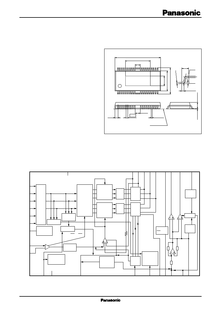
Block Diagram
Unit: mm
HSOP042-P-0400C
(1.315)
0
∞
to 10
∞
0.5±0.2
0.30
+0.10
≠ 0.05
(1.95)
1
9
13
21
42
34
30
22
(10.00)
18.4±0.2
2.7±0.2
0.1±0.1
(1.20)
+0.10
≠ 0.05
0.35
0.80
(3.20)
Seating plane
8.3±0.2
10.93±0.30
(4.00)
10
7
4
9
32
35
36
34
V
CC2
det
.
Reset
V
REF
det.
29
VM1
CS
A1
A2
A3
VM2
VN
VP
V
CC2
1
2
VM2
FIN1
15
14
12
1
2
11
5
28
22
25
26
27
23
21
20
19
18
16
17
Hall
bias
Start/stop
Thermal
protection
circuit
Absolute
value
Brake
circuit
Hall
amp.
matrix
Detection
Upper side
distribution
Upper
side
power
Lower
side
power
Lower side
distribution
Logic
Amp.
Amp.
Direction
detection
Direction
changeover
EA
ER
VTL
S/S
V
CC1
PCI
BRK
PG1
PG2
SLIN
PC
FG
V
REF
H1
+
H1
-
H2
+
H2
-
H3
+
H3
-
VH
EC
ECR
SG
EP
=
ER
◊
EA
FG
comparator

AN8488SB
ICs for Compact Disc/ CD-ROM Player
2
s
Pin Descriptions
s
Absolute Maximum Ratings
Parameter
Symbol
Rating
Unit
Supply voltage
V
CC1
7.0
V
V
CC2
14.0
V
M1
, V
M2
Output voltage 1
*4
V
O1(n)
-
0.3 to V
M1
+
0.4
V
Output voltage 2
*5
V
O2(n)
-
0.3 to V
M2
+
0.4
V
Control signal input voltage
*4
V
(n)
0 to V
CC1
V
Supply current
I
CC1
30
mA
Output current
*3
I
O(n)
±
1 200
mA
Hall bias current
I
HB
50
mA
Power dissipation
*2
P
D
786
mW
Operating ambient temperature
*1
T
opr
-
20 to
+
75
∞
C
Storage temperature
*1
T
stg
-
55 to
+
150
∞
C
Note) Do not apply external currents or voltages to any pins not specifically mentioned.
For circuit currents, '
+
' denotes current flowing into the IC, and '
-
' denotes current flowing out of the IC.
*1: Except for the operating ambient temperature and storage temperature, all ratings are for T
a
=
25
∞
C.
*2: The power dissipation shown is the value of independent IC without a heat sink at T
a
=
75
∞
C. Refer to the P
D
T
a
curves
of the "s Application Notes" for details.
Pin No. Symbol
Description
19
H2
-
Hall element-2 negative input pin
20
H3
+
Hall element-3 positive input pin
21
H3
-
Hall element-3 negative input pin
22
V
CC1
SPD block supply voltage pin
23
VH
Hall bias pin
24
N.C.
N.C.
25
SS
Start/stop changeover pin
26
ECR
Torque command reference input pin
27
EC
Torque command input pin
28
PCI
Current feedback phase compensation pin
29
VM1
SPD block motor supply voltage pin
30
N.C.
N.C.
31
N.C.
N.C.
32
A3
A3 phase output pin
33
N.C.
N.C.
34
CS
Current det. pin
35
A2
A2 phase output pin
36
A1
A1 phase output pin
FIN2
Pin No. Symbol
Description
1
PG1
SPD block power GND pin
2
PG2
Driver block power GND pin
3
N.C.
N.C.
4
VN
Driver block inverted output pin
5
PC
Driver block power cut pin
6
N.C.
N.C.
7
VP
Driver block forward output pin
8
N.C.
N.C.
9
VM2
Driver block motor power supply pin
10
V
CC2
Driver block supply voltage pin
11
SLIN
Driver block input pin
12
V
REF
Driver block reference input pin
13
N.C.
N.C.
14
FG
FG signal output pin
15
BRK
Brake mode setting pin
16
H1
+
Hall element-1 positive input pin
17
H1
-
Hall element-1 negative input pin
18
H2
+
Hall element-2 positive input pin
FIN1
SG
Signal GND pin

ICs for Compact Disc/ CD-ROM Player
AN8488SB
3
s
Electrical Characteristics at T
a
=
25
∞
C
Parameter
Symbol
Conditions
Min
Typ
Max
Unit
Overall
Circuit current 1
I
CC1
V
CC1
=
5 V, SS: at low
0
0.1
mA
Circuit current 2
I
CC2
V
CC2
=
12 V, SS: at low
60
200
µ
A
Start/stop
Start voltage
V
START
Voltage with which a circuit operates
2.7
V
at V
CC1
=
5 V and L
H
Stop voltage
V
STOP
Voltage with which a circuit becomes
0.7
V
off at V
CC1
=
5 V and H
L
Medium voltage
V
MED
Voltage with which V
PC1
becomes
1.425
1.65
1.89
V
low at V
CC1
=
5 V and EC
=
0 V
<Spindle block>
Hall bias
Hall bias voltage
V
HB
V
CC1
=
5 V, I
HB
=
20 mA
0.7
1.2
1.6
V
Hall amplifier
Input bias current
I
BH
V
CC1
=
5 V
1
5
µ
A
In-phase input voltage range
V
HBR
V
CC1
=
5 V
1.5
4.0
V
Minimum input level
V
INH
V
CC1
=
5 V
60
mV[p-p]
Torque command
In-phase input voltage range
EC
V
CC1
=
5 V
0.5
3.9
V
Offset voltage
EC
OF
V
CC1
=
5 V
-
100
0
100
mV
Dead zone
EC
DZ
V
CC1
=
5 V
25
75
125
mV
Input current
EC
IN
V
CC1
=
5 V, EC
=
ECR
=
1.65 V
-
5
-
0.25
µ
A
Input/output gain
A
CS
V
CC1
=
5 V, R
CS
=
0.6
0.75
1.0
1.25
A/V
Output
High-level output saturation voltage
V
OH
V
CC1
=
5 V, I
O
=
-
300 mA
0.9
1.6
V
Low-level output saturation voltage
V
OL
V
CC1
=
5 V, I
O
=
300 mA
0.2
0.6
V
Torque limit current
I
TL
V
CC
=
5 V, R
CS
=
0.6
400
500
600
mA
s
Absolute Maximum Ratings (continued)
Note) *3: n
=
4, 7, 32, 35, 36
*4: n
=
32, 35, 36
*5: n
=
4, 7
*6: n
=
5, 11, 12, 15, 25, 26, 27
s
Recommended Operating Range
Parameter
Symbol
Range
Unit
Supply voltage
V
CC1
4.25 to 5.5
V
V
CC2
4.5 to 13.5
V
M1
, V
M2

AN8488SB
ICs for Compact Disc/ CD-ROM Player
4
s
Electrical Characteristics at T
a
=
25
∞
C (continued)
Parameter
Symbol
Conditions
Min
Typ
Max
Unit
<Spindle block> (continued)
FG
FG output high-level
FG
H
V
CC1
=
5 V, I
FG
=
-
0.01 mA
3.0
V
CC1
V
FG output low-level
FG
L
V
CC1
=
5 V, I
FG
=
0.01 mA
0.5
V
In-phase input voltage range
V
FGR
V
CC1
=
5 V,
1.5
3.0
V
Input D-range at H2
+
, H2
-
FG hysteresis width
H
FG
V
CC1
=
5 V
1
10
20
mV
Brake cirrcuit
Short brake model level
V
SBR
V
CC1
=
5 V
1.0
V
Reverse rotation brake mode level
V
RBR
V
CC1
=
5 V
3.5
V
Short brake start level
V
SBRL
V
CC1
=
5 V, ECR
=
1.65 V
1.65
1.74
V
Short brake current
I
SBR
V
CC1
=
5 V
60
90
mA
<Driver block>
Driver
R
L
=
16
Output offset voltage
V
DROF
SL IN
=
1.65 V
-
150
0
+
150
mV
+
gain
G
SL
+
R IN
= 10
k
21
23
25
dB
+
/
-
relative gain
G
SL
-
0.7
0
+
0.7
dB
Output D range '
+
'
V
O
+
SL IN
=
3.3 V
9.3
10.0
V
Output D range '
-
'
V
O
-
SL IN
=
0 V
-
10.0
-
9.3
V
Power cut operation
High-level PC threshold voltage
V
PCH
V
CC2
=
12 V
2.9
V
Low-level PC threshold voltage
V
PCL
V
CC2
=
12 V
1.0
V
PC input current
I
PC
V
CC2
=
12 V, PC
=
5 V
100
200
µ
A
Reset cirrcuit
Reset operation release supply voltage
V
RST
4.5
V
V
REF
detection voltage
V
R
1.35
∑
Design reference data
Note) The characteristics listed below are theoretical values based on the IC design and are not guaranteed.
Parameter
Symbol
Conditions
Min
Typ
Max
Unit
Thermal protection
Thermal protection operating
T
SDON
V
CC1
=
5 V
160
∞
C
temperature
Thermal protection hysteresis width
T
SD
V
CC1
=
5 V
45
∞
C
Sled block supply voltage
Sled block supply voltage detection
V
HD
0.2
V
hysteresis width
ICs for Compact Disc/ CD-ROM Player
AN8488SB
5
s
Usage Notes
1. Use the V
CC2
at V
CC2
V
M2
. And use power supply always at on state. Otherwise it will cause malfunction.
2. On driver gain setting of driver block.
Voltage gain of power amplifier: 23 dB
3. On operation mode of mute:
11
4
7
10 k
10 k
500
5.5 k
V
REF
V
REF
Input
Input pin
M
◊
7
◊
7
Power amp. Output pin
Load
4. On SS pin mode:
PC
H
L (Open)
Driver output
Active
Mute
6. Take time to check the characteristics on use.
When changing an external circuit constant for use, consider not only static characteristics, but also transient charac-
teristics and external parts with respect to the characteristics difference among ICs so that you can get enough margin.
7. Avoid short-circuit between output pin and power supply, output pin and GND (line-to-supply and line-to-ground
fault) and output pins (load short-circuit). Otherwise the IC will be damaged and is likely to get fired.
8. Be cautious on a dip soldering. Prior study is required.
SS
H
M
L (Open)
Spindle block
On
Off
Off
Driver block
On
On
Off
5. On brake mode of spindle block:
BRK
H
L (Open)
EC
<
ECR
Acceleration
Acceleration
EC
>
ECR
Reverse rotation brake
Short brake

AN8488SB
ICs for Compact Disc/ CD-ROM Player
6
∑
Phase conditions between Hall input and output current
s
Application Notes
∑
P
D
T
a
curves of HSOP042-P-0400
P
D
T
a
0.000
0
25
50
75
100
125
150
3.000
2.723
2.500
2.000
1.500
1.311
1.000
0.500
786 mW
1 634 mW
Mounted on standard board
(glass epoxy: 75
◊
75
◊
t0.8 mm
3
)
R
th(j-a)
=
45.9
∞
C/W
Independent IC
without a heat sink
R
th(j-a)
=
95.3
∞
C/W
Po
wer dissipation
P
D
(W)
Ambient temperature T
a
(
∞
C)
A
B
C
D
E
F
Phase of Hall pin
H1
+
H3
+
H2
+
H
M
L
H
M
L
M
L
H
L
M
H
L
M
H
M
L
H
ECR
EC
A
B
C
D
E
H1
H2
H2
H1
H3
H3
A3
A3
A2
A1
A2
A1
F
0
0
0
Emit
Output current
Sink

ICs for Compact Disc/ CD-ROM Player
AN8488SB
7
s
Application Notes (continued)
∑
Power consumption calculation method
You can find a rough value of electric power to be consumed in the IC in the following method and the use of EXCEL
(computer soft ware) will enable you to put it on a graph.
Calculating formula:
(Spindle block)
1. Let an induced voltage generated in each phase as below:
(Reference to a motor center point)
E
A1
=
E
O
◊
sin (X) ∑ ∑ ∑ (1)
E
A2
=
E
O
◊
sin (X
+
120) ∑ ∑ ∑ (2)
E
A3
=
E
O
◊
sin (X
+
240) ∑ ∑ ∑ (3)
X: Phase angle
2. Let a current flowing in each phase as below:
I
A1
=
I
O
◊
sin (X) ∑ ∑ ∑ (4)
I
A2
=
I
O
◊
sin (X
+
120) ∑ ∑ ∑ (5)
I
A3
=
I
O
◊
sin (X
+
240) ∑ ∑ ∑ (6)
3. The voltages generated by a wire-wound resistance of a motor are:
V
R1
=
I
A1
◊
R ∑ ∑ ∑ (7)
V
R2
=
I
A2
◊
R ∑ ∑ ∑ (8)
V
R3
=
I
A3
◊
R ∑ ∑ ∑ (9)
4. In each phase, add the voltage generated by an induced voltage and that by a wire-wound resistance.
V
A1
'
=
(1)
+
(4)
V
A2
'
=
(2)
+
(5)
V
A3
'
=
(3)
+
(6)
5. As the lowest voltage in each phase angle must be 0 V, you can get the voltage to be generated in each phase by
means of subtracting the lowest voltage from the voltage of the remaining two phases.
V
A1
=
V
A1
'
-
MIN (V
A1
', V
A2
', V
A3
') ∑ ∑ ∑ (10)
V
A2
=
V
A2
'
-
MIN (V
A1
', V
A2
', V
A3
') ∑ ∑ ∑ (11)
V
A3
=
V
A3
'
-
MIN (V
A1
', V
A2
', V
A3
') ∑ ∑ ∑ (12)
6. Subtract the supply voltage from each phase's voltage found in item 5 and then multiply it by each phase's current,
so that you can get the power consumption of the spindle block.
3
P
SPD
=
(
12
-
V
An
) ◊
I
An
n
=
1
(Driver block)
P
SL
=
(V
M2
-
I
O
∑ R)
◊
I
O
V
M2
: Motor power supply voltage
I
O
: Output current
R: Wire wound resistor
∑
Theory of thermal resistance
A chip temperature or the fin temperature can be understood in the same way as Ohm's Law.
T
j
: Chip temperature
T
a
: Ambient temperature
P
: Electric power generated by IC
R
j-c
: Thermal resistance between a chip and a package
R
c-a
: Thermal resistance between a package and a surface of a heat sink or free air
T
j
=
T
a
+
P
◊
(R
j-c
+
R
c-a
)
Make sure that T
j
does not exceed 150
∞
C.
If it exceeds 150
∞
C, you can suppress the rise of a chip temperature by adding a heat sink which is equivalent to
R
f
in the above figure.
T
j
=
T
a
+
P
◊
(R
j-c
+
R
c-a
)
A package surface and the fin are available for a temperature measurement. But the fin part is recommendable for
measurement because a package surface measurement does not always promise you a consistent measuring result.
Note) What has been mentioned above is true to a stationary state, not to a transient state.
R
f
T
j
R
j-c
R
c-a
T
a
P

AN8488SB
ICs for Compact Disc/ CD-ROM Player
8
s
Application Circuit Example
S/S: High: SPD block on and driver block on
Med: SPD block off and driver block on
Low: SPD block off and driver block off
10
7
4
9
32
35
36
34
V
CC2
det
.
Reset
V
REF
det.
29
VM2
V
CC2
1
2
VM2
FIN1
15
14
12
1
2
11
5
28
22
25
26
27
23
21
20
19
18
16
17
Hall
bias
Start/stop
Thermal
protection
circuit
Absolute
value
Brake
circuit
Hall
amp.
matrix
Detection
Upper side
distribution
Upper
side
power
Lower
side
power
Lower side
distribution
Logic
Amp.
Amp.
Direction
detection
Direction
changeover
EA
ER
VTL
FG
comparator
H1
+
H1
-
H2
+
H2
-
H3
+
H3
-
VH
EC
ECR
Servo
torque
command
SLIN
Low: Short brake
High: Reverse rotation break
FG signal
V
CC
=
5 V
R
IN
=
10 k
0.1
µ
F
S/S
V
CC1
PCI
BRK
PG1
PG2
SLIN
PC
FG
V
REF
VM1
VM1
=
12 V
SG
CS
A1
A2
A3
VN
VP
M
R
CS
=
0.6
EP
=
ER
◊
EA