ICs for Mobile Communication
1
AN8539SH
300 MHz-band single PLL IC
s
Overview
The AN8539SH is a 300 MHz-band, 2nd local
OSC PLL IC designed for a cellular phone which
allows IF switching to high or low.
s
Features
∑
To be switched to two frequencies.
(Select by SELECT pin.)
∑
Analog SW built-in
∑
I
CC
=
900
µ
A
s
Applications
∑
Cellular phone
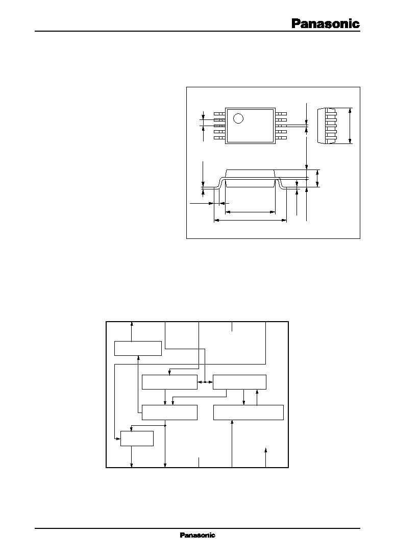
SSOP010-P-0225
Unit: mm
4.3±0.30
6.3±0.30
0.5±0.2
0.1±0.1
1
5
10
6
0.2±0.1
0.5
3.0±0.30
1.5±0.2
0.625±0.10
0.625±0.10
0.15
+0.1
≠0.05
s
Block Diagram
10
9
8
7
6
1
LD
SELECT
REF
V
CC
SW
2
3
4
5
14-bit R counter
Phase comparator
Selector
Lock detection
15-bit N counter
1/16, 1/17 prescaler
PS
IFIN
GND
CP
CPSUB
AN8539SH
ICs for Mobile Communication
2
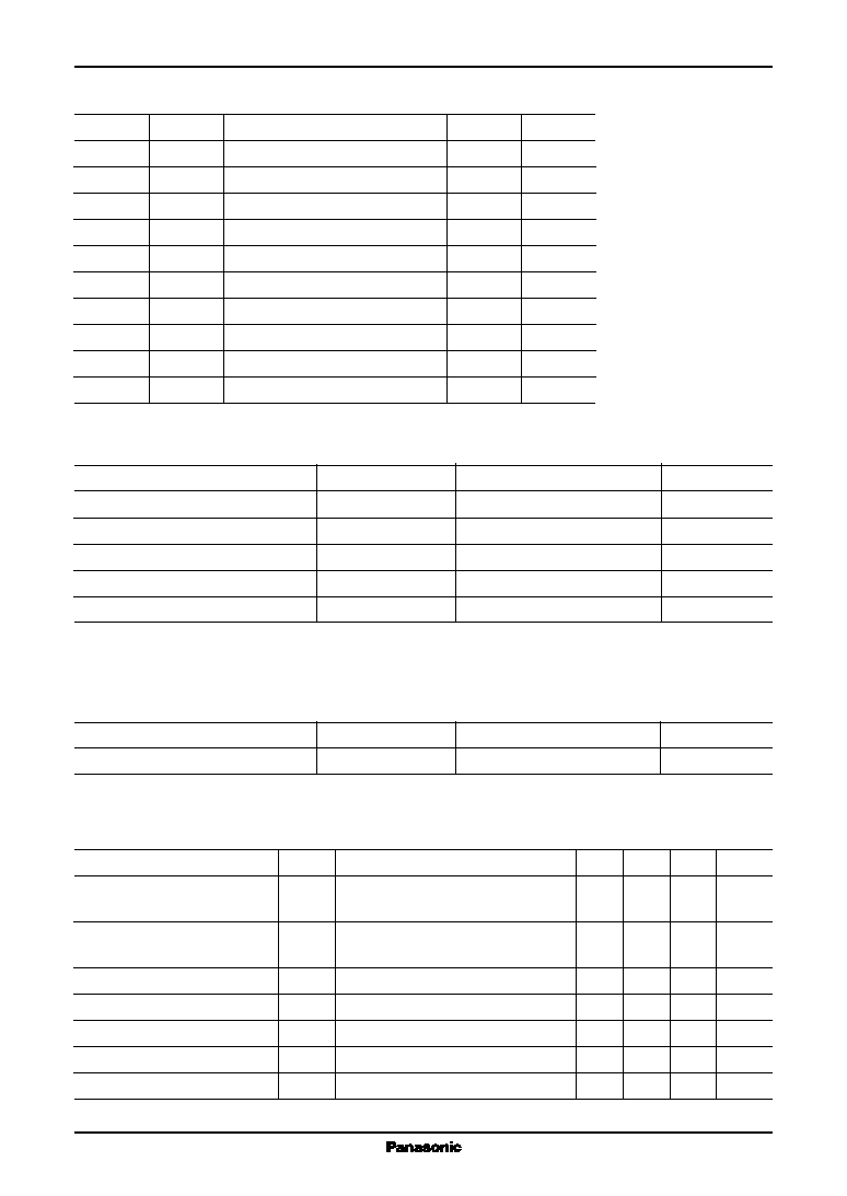
Parameter
Symbol
Range
Unit
Supply voltage
V
CC
2.55 to 3.3
V
s
Recommended Operating Range
s
Pin Descriptions
Parameter
Symbol
Rating
Unit
Supply voltage
V
CC
3.6
V
Supply current
I
CC
3.5
mA
Power dissipation
*2
P
D
12.6
mW
Operating ambient temperature
*1
T
opr
-
30 to
+
85
∞C
Storage temperature
*1
T
stg
-
55 to
+
125
∞C
s
Absolute Maximum Ratings
Note) *1: Except for the operating ambient temperature and storage temperature, all ratings are for T
a
=
25
∞
C.
*2: T
a
=
85
∞
C
Pin No.
Symbol
Description
I/O
Level
1
CPSUB
Sub charge pump output
O
CMOS
2
CP
Charge pump output
O
CMOS
3
GND
GND pin
4
IFIN
IF input
I
ECL
5
PS
Power save control
I
CMOS
6
SW
Sub charge pump control
I
CMOS
7
V
CC
Power supply pin
8
REF
Reference frequency input
I
ECL
9
SELECT
IF frequency changeover control
I
CMOS
10
LD
Lock detection output
O
CMOS
s
Electrical Characteristics at V
CC
=
2.7 V, f
REFIN
=
12.8 MHz, V
REFIN
=
0.6 V[p-p], T
a
=
25
∞
C
Parameter
Symbol
Conditions
Min
Typ
Max
Unit
Consumption current 1
I
CC1
SELECT
=
high
0.90
1.21
mA
At 178 MHz lock
Consumption current 2
I
CC2
Power save mode
0
10
µ
A
At PS
=
GND setting
Reference signal input level
V
REFIN
f
REFIN
=
12.8 MHz
0.5
1.2
V[p-p]
High-level input voltage
V
IH
2.16
3.30
V
Low-level input voltage
V
IL
0
0.54
V
High-level input current
I
IH
At V
IH
=
2.16 V applied
-
1
0
1
µ
A
Low-level input current
I
IL
At V
IL
=
0 V applied
-
1
0
1
µ
A
ICs for Mobile Communication
AN8539SH
3
s
Electrical Characteristics at V
CC
=
2.7 V, f
REFIN
=
12.8 MHz, V
REFIN
=
0.6 V[p-p], T
a
=
25
∞
C
(continued)
∑
Design reference data at T
a
=
-
30
∞
C to 80
∞
C
Note) The characteristics listed below are theoretical values based on the IC design and are not guaranteed.
Parameter
Symbol
Conditions
Min
Typ
Max
Unit
Consumption current 1
I
CC1
SELECT
=
high, at 178 MHz lock
0.90
1.34
mA
Consumption current 2
I
CC2
SELECT
=
low, at 129.55 MHz lock
0.83
1.27
mA
IF input level
V
IFIN
f
IFIN
=
100 MHz to 350 MHz
-
10
+
2
dBm
Reference signal input level
V
REFIN
f
REFIN
=
10 MHz to 25 MHz
0.5
1.2
V[p-p]
Output leak current
I
OZ
At V
OZ
=
0 V, 2.7 V applied
-
1.0
+
1.0
µ
A
Charge pump output current 1
I
OH
At V
OH
=
2.16 V applied
-
0.67
-
0.48
-
0.30
mA
Charge pump output current 2
I
OL
At V
OL
=
0.54 V applied
0.32
0.51
0.72
mA
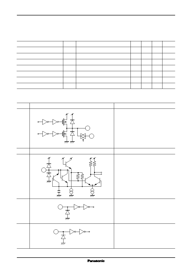
Pin No.
Equivalent circuit
Description
1
Pin 1: CPSUB
2
Pin 2: CP
3
GND
4
IFIN input
5
PS input
6
SW input
s
Terminal Equivalent Circuits
2 CP
CPSUB
1
SW
4
4.5 k
4.5 k
Pin 5
9
6
AN8539SH
ICs for Mobile Communication
4
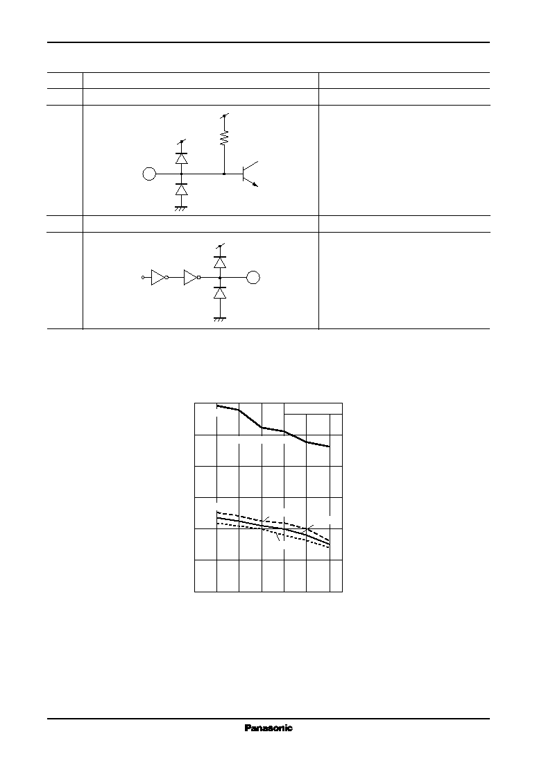
Pin No.
Equivalent circuit
Description
7
V
CC
8
REF
9
Refer to pin 5
SELECT inpuit
10
LD output
s
Terminal Equivalent Circuits (continued)
10 k
8
10
s
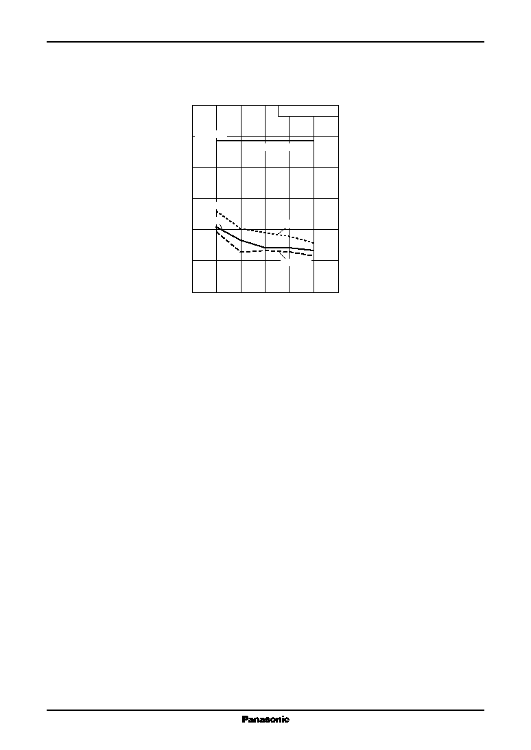
Application Notes
1. Input level characteristics
1) IF input level characteristics
Input frequency (MHz)
Input level
(dBm)
-
40
-
30
-
20
-
10
0
10
50
100
150
200
250
300
350
T
a
=
85
∞
C
T
a
=
-
30
∞
C, 25
∞
C, 85
∞
C
T
a
=
25
∞
C
V
CC
=
2.55 V to 3.3V
Upper limit
Lower limit
T
a
= -
30
∞
C
ICs for Mobile Communication
AN8539SH
5
s
Application Notes (continued)
1. Input level characteristics (continued)
2) REF input level characteristics
Input frequency (MHz)
Input level
(dBm)
-
30
-
20
-
10
0
10
20
0
5
10
15
20
25
30
T
a
=
85
∞
C
T
a
=
-
30
∞
C, 25
∞
C, 85
∞
C
T
a
=
25
∞
C
V
CC
=
2.55 V to 3.3V
T
a
= -
30
∞
C
Upper limit
Lower limit
2. Characteristics specification
1) IF select specification
SELECT pin control enables you to switch IF as below:
SELECT
=
low
f
OUT
=
129.55 MHz, f
R
=
50 kHz (P
=
16, N
=
161, A
=
15, R
=
256)
SELECT
=
high
f
OUT
=
178 MHz, f
R
=
400 kHz (P
=
16, N
=
27, A
=
13, R
=
32)
2) Unlock detection and LD output specification
LD output is high in a lock mode and low in an unlock mode. Lock signal is outputted in a power save mode.
SELECT
=
high : Detection time is 2.6
µ
s. About detection accuracy, when a dividing output shifts
by
±
(78
◊
3) ns for f
REF
=
400 kHz, it generates an unlock output.
SELECT
=
low : Detection time is 20
µ
s. About detection accuracy, when a dividing output shifts
by
±
(78
◊
3) ns for f
REF
=
50 kHz, it generates an unlock output.
3) Power save control specification
When power save control pin (PS) is high, it is set to an operating mode. When it is low, it is set to power save mode.
4) Analog SW control specification
CPSUB is controlled by SW pin.
SW
=
low : CPSUB open
SW
=
high: CPSUB operation
5) Other specification
Set CMOS input pins, such as PS pin, SW pin, SELECT pin, etc., normally to V
CC
or GND.