 | –≠–ª–µ–∫—Ç—Ä–æ–Ω–Ω—ã–π –∫–æ–º–ø–æ–Ω–µ–Ω—Ç: AN8612NSB | –°–∫–∞—á–∞—Ç—å:  PDF PDF  ZIP ZIP |
ICs for Information Equipment
1
AN8612NSB
SCSI active terminator IC
s
Overview
The AN8612NSB is a terminator IC conformed
to standard interface specification (SCSI-I/II) for
personal computers, workstations and various types
of information equipment. So far configured with
a fixed resistor and a regulator, it has recently been
integrated onto a single chip with built-in standby
function.
It is easy to satisfy 25 pF of the maximum pin
capacitance in SCSI-II specification due to its small
output pin capacitance. It can sapport 10 Mbyte/s of
SCSI-II and 20 Mbyte/s of FAST-20.
s
Features
∑
Active termination for 18-signal line
∑
Low power consumption due to its standby func-
tion (100
µ
A at standby).
∑
Small output pin capacitance: 3.8 pF (typ.)
∑
High precision regulator: 2.85 V
±
60 mV
s
Applications
∑
SCSI interface board of PC
∑
SCSI-compatible equipment such as CD-ROM,
MO, PD, MD drive and printer
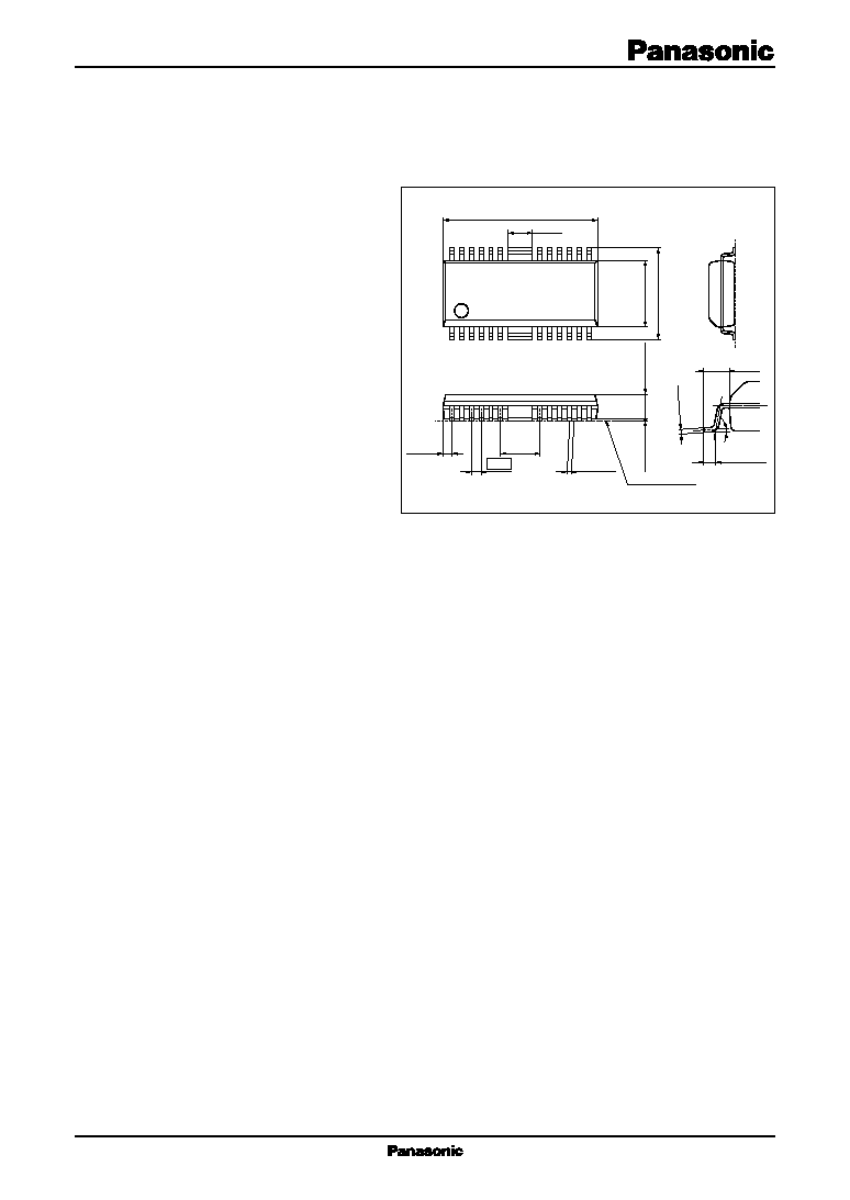
HSOP030-P-0300
Unit: mm
12.63±0.20
(1.90)
(1.05)
0.50±0.20
0
∞
to 10
∞
24
19
18
13
1
6
7
(0.715)
(3.20)
0.10±0.10
2.00±0.20
7.60±0.30
5.50±0.20
0.30
+0.10
≠0.05
12
0.80
Seating plane
0.20
+0.10
≠0.05
AN8612NSB
ICs for Information Equipment
2
s
Block Diagram
24
18
115
REG out
SG line1
17
115
SG line2
16
115
SG line3
15
115
SG line4
14
115
SG line5
11
115
SG line6
10
115
SG line7
9
115
SG line8
8
115
SG line9
7
115
SG line10
5
115
SG line11
4
115
Thermal
shut down
SG line12
3
115
SG line13
2
115
SG line14
23
115
SG line15
22
115
SG line16
21
115
SG line17
20
1
6
GND
115
SG line18
Standby
12
13
TERMPWR
2.85 V
Band gap
reference
19
GND
ICs for Information Equipment
AN8612NSB
3
s
Pin Descriptions
Pin No.
Description
1
Standby
*1
2
SG line14
3
SG line13
4
SG line12
5
SG line11
6
GND
*2
Fin
GND
*2
7
SG line10
8
SG line9
9
SG line8
10
SG line7
11
SG line6
12
V
CC
(TERMPWR)
*3
Pin No.
Description
13
V
CC
(TERMPWR)
*3
14
SG line5
15
SG line4
16
SG line3
17
SG line2
18
SG line1
Fin
GND
*2
19
GND
*2
20
SG line18
21
SG line17
22
SG line16
23
SG line15
24
REG out
Note) *1: A standby pin input voltage becomes an active mode at V
I
<
V
TH
and a standby mode at V
I
>
V
TH
+
.
Likewise, a standby mode when standby pin is open.
*2: Both ground pins of the pin 6 and pin 19 should be placed on the same pattern, and the pattern should be wide on the PCB.
(We recommend that whole surface of one layer of a multi-layer PCB be GND.)
*3: Connect the V
CC
to SCSI termination resistor power supply (TERMPWR).
Parameter
Symbol
Range
Unit
Supply voltage
V
CC
4.0 to 5.5
V
s
Recommended Operating Range
Parameter
Symbol
Rating
Unit
Supply voltage
V
CC
6.0
V
Supply current
I
CC
550
mA
Power dissipation
*2
P
D
412
mW
Operating ambient temperature
*1
T
opr
-
20 to
+
75
∞C
Storage temperature
*1
T
stg
-
55 to
+
150
∞C
s
Absolute Maximum Ratings
Note) *1: Except for the power dissipation, operating ambient temperature and storage temperature, all ratings are for T
a
=
25
∞
C.
*2: T
a
=
75
∞
C. For the independent IC without a heat sink.
Refer to "s Application Notes".
AN8612NSB
ICs for Information Equipment
4
s
Electrical Characteristics at V
CC
=
5.0 V, T
a
=
25
∞
C
Parameter
Symbol
Conditions
Min
Typ
Max
Unit
Supply current 1
I
CC1
Standby
=
low, all SG line
=
open
44
54
mA
Supply current 2
I
CC2
Standby
=
low, All SG line
=
0.2 V
458
530
mA
Supply current 3
I
CC3
Standby
=
open
100
200
µ
A
Standby pin low-level input
I
STBYL
V
CC
=
5.5 V, V
I
=
0 V
-
150
-
50
µ
A
current
Standby pin high-level input
I
STBYH
V
CC
=
5.5 V, V
I
=
5.5 V
1
µ
A
current
Standby pin positive direction
V
TH
+
1.3
1.5
1.7
V
threshold voltage
Standby pin negative direction
V
TH
-
1.1
1.3
1.5
V
threshold voltage
Maximum output current
I
SG
V
SG
=
0.2 V
19.8
23.0
26.2
mA
SG line1 to SG line18
Output leak current 1
I
LK1
V
CC
=
5.5 V
-
1
µ
A
SG line1 to SG line18
Standby
=
open, V
SG
=
0 V
Output leak current 2
I
LK2
V
CC
=
5.5 V, V
SG
=
2.85 V
-
1
1
µ
A
SG line1 to SG line18
Standby
=
open
REG output voltage 1
V
REG1
V
CC
=
4.0 V to 5.5 V, all SG line
=
open
2.79
2.85
2.91
V
REG output voltage 2
V
REG2
V
CC
=
3.2 V, all SG line
=
open
2.00
V
Termination resistance value
R
SG
I
SG
=
5 mA to 15 mA
107
115
123
SG line1 to SG line18
High-level output voltage
V
SGH
V
CC
=
4.0 V to 5.5 V, all SG line
=
open
2.78
2.85
2.92
V
SG line1 to SG line18
∑
Design reference data
Note) The characteristics listed below are theoretical values based on the IC design and are not guaranteed.
Parameter
Symbol
Conditions
Min
Typ
Max
Unit
Standby pin hysteresis width
V
HYS
200
mV
Output pin capacitance
C
SG
3.8
4.5
pF
Thermal shutdown temperature
T
TSD
170
∞
C
Pin No.
Symbol
Equivalent circuit
1
Standby
s
Terminal Equivalent Circuits
100 k
V
CC
GND
1
ICs for Information Equipment
AN8612NSB
5
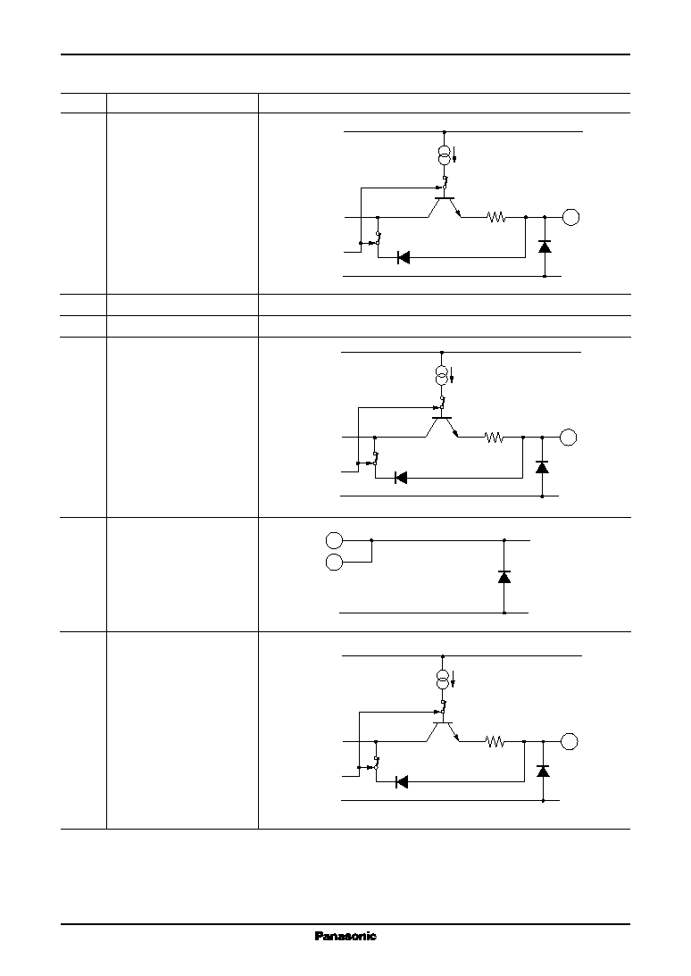
Pin No.
Symbol
Equivalent circuit
2
Pin 2: SG line14
3
Pin 3: SG line13
4
Pin 4: SG line12
5
Pin 5: SG line11
6
GND
Fin
GND
7
Pin 7: SG line10
8
Pin 8: SG line9
9
Pin 9: SG line8
10
Pin 10: SG line7
11
Pin 11: SG line6
12
Pin 12: V
CC
(TERMPWR)
13
Pin 13: V
CC
(TERMPWR)
14
Pin 14: SG line5
15
Pin 15: SG line4
16
Pin 16: SG line3
17
Pin 17: SG line2
18
Pin 18: SG line1
s
Terminal Equivalent Circuits (continued)
115
V
CC
REG out
Standby
GND
Pin 2
3
4
5
115
V
CC
REG out
Standby
GND
Pin 7
8
9
10
11
GND
12
13
115
V
CC
REG out
Standby
GND
Pin 14
15
16
17
18