 | ÐлекÑÑоннÑй компоненÑ: AN8814 | СкаÑаÑÑ:  PDF PDF  ZIP ZIP |
Äîêóìåíòàöèÿ è îïèñàíèÿ www.docs.chipfind.ru
ICs for Compact Disc/CD-ROM Player
1
AN8814SB
4-channel driver IC for optical disk drive
s
Overview
The AN8814SB is a BTL system 4-channel
driver and is encapsulated in the SMD package
which excels in heat radiation characteristic.
s
Features
·
Wide output dynamic range regardless of refer-
ence voltage of the system
·
Driver I/O gain setting is possible with an addi-
tional external resistor
·
3.3 V supply voltage is available due to an exter-
nal PNP-tr.
·
Additional OP-amp. built-in
s
Applications
·
MD, CD/CD-ROM drive
·
DVD/DVD-ROM drive
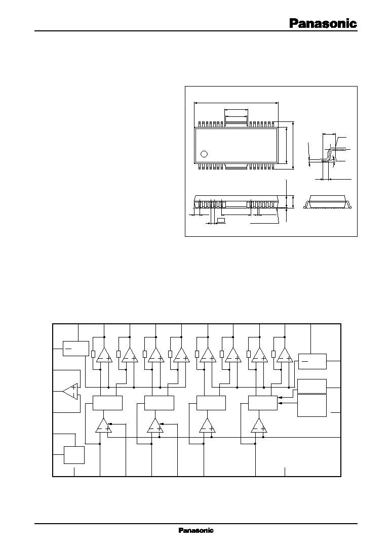
HSOP042-P-0400
Unit: mm
1
7
8
14
(1.315)
0.65±0.20
28
22
21
(4.8)
(6.4)
(1.2)
(5.15)
18.4±0.2
8.3±0.2
2.7±0.2
0.1±0.1
10.93±0.30
15
0.35
+0.10
0.05
0.30
+0.10
0.05
0.8
Seating plane
0
°
to 10
°
s
Block Diagram
19
PGND1
20
PV
CC1
23
IN1
18
VO1
+
24
PC1
17
VO1
-
25
IN2
16
VO2
+
26
PC2
15
VO2
-
27
IN3
14
VO3
+
13
VO3
-
28
IN4
12
VO4
+
10
PGND2
11
VO4
-
9
PV
CC2
21
8
6
7
V
CC
4
Fin
GND
5
V
CC
22
V
REF
1
2
PV
CC
1
2
PV
CC
1
2
3.3 V
reg.
Direction
detector
Direction
detector
Direction
detector
Direction
detector
V
CC
detector
Thermal
protection
circuit

AN8814SB
ICs for Compact Disc/CD-ROM Player
2
Pin No.
Description
15
Motor driver-2 reverse rotation output pin
16
Motor driver-2 forward rotation output pin
17
Motor driver-1 reverse rotation output pin
18
Motor driver-1 forward rotation output pin
19
Driver GND pin 1
20
Driver power supply pin 1
21
1/2 PV
CC
output pin 1
22
V
REF
input pin
23
Motor driver-1 input pin
24
PC (power cut) input pin 1
25
Motor driver-2 input pin
26
PC (power cut) input pin 2
27
Motor driver-3 input pin
28
Motor driver-4 input pin
Fin
GND pin
s
Pin Descriptions
Pin No.
Description
1
Base control pin for an external transistor
of 3.3 V regulator
2
3.3 V regulator output monitor pin
3
N.C. pin
4
Op-amp. output pin
5
Op-amp. inverted input pin
6
Op-amp. non-inverted input pin
7
Power supply pin
8
1/2 PV
CC
output pin 2
9
Driver power supply pin 2
10
Driver GND pin 2
11
Motor driver-4 reverse rotation output pin
12
Motor driver-4 forward rotation output pin
13
Motor driver-3 reverse rotation output pin
14
Motor driver-3 forward rotation output pin
Parameter
Symbol
Range
Unit
Supply voltage
SV
CC
, PV
CC1
, PV
CC2
4.0 to 14
V
s
Recommended Operating Range
Parameter
Symbol
Rating
Unit
Supply voltage
SV
CC
17
V
Supply current
I
CC
mA
Power dissipation
*2
P
D
542
mW
Operating ambient temperature
*1
T
opr
-
30 to
+
85
°C
Storage temperature
*1
T
stg
-
55 to
+
150
°C
s
Absolute Maximum Ratings
Note) *1: Except for the operating ambient temperature and storage temperature, all ratings are for T
a
=
25
°
C.
*2: T
a
=
85
°
C.
Referring to "s Application Circuit Example", following the allowable power dissipation characteristic curve of "s
Application Notes".

ICs for Compact Disc/CD-ROM Player
AN8814SB
3
s
Electrical Characteristics at T
a
=
25
°
C
Parameter
Symbol
Conditions
Min
Typ
Max
Unit
Current consumption with no load
I
TOT
V
CC
=
5 V
5
10
15
mA
Motor driver 1 to motor driver 4
Input offset voltage
V
IOF
V
CC
=
5 V, V
PC1
=
V
PC2
=
0 V,
-
10
0
10
mV
R
L1
to R
L4
= 8
k
, R
1
to R
4
= 10
k
Output offset voltage
V
OOF
V
CC
=
5 V, V
PC1
=
V
PC2
=
0 V,
-
50
0
50
mV
R
L1
to R
L4
= 8
k
, R
1
to R
4
= 10
k
Gain
G
V
CC
=
5 V, V
PC1
=
V
PC2
=
0 V,
18.0
20.0
22.0
dB
R
L1
to R
L4
= 8
k
, R
1
to R
4
= 10
k
Maximum output amplitude (
+
)
V
L
+
V
CC
=
5 V, V
PC1
=
V
PC2
=
0 V,
2.4
2.7
V
R
L1
to R
L4
= 8
k
, R
1
to R
4
= 10
k
Maximum output amplitude (
-
)
V
L
-
V
CC
=
5 V, V
PC1
=
V
PC2
=
0 V,
-
2.7
-
2.4
V
R
L1
to R
L4
= 8
k
, R
1
to R
4
= 10
k
Motor driver 1
High-level threshold voltage
V
PCH1
V
CC
=
5 V, R
L1
=
8
, R
1
=
10 k
2.0
V
Low-level threshold voltage
V
PCL1
V
CC
=
5 V, R
L1
=
8
, R
1
=
10 k
0.5
V
Motor driver 2
High-level threshold voltage
V
PCH2
V
CC
=
5 V, R
L2
=
8
, R
2
=
10 k
2.0
V
Low-level threshold voltage
V
PCL2
V
CC
=
5 V, R
L2
=
8
, R
2
=
10 k
0.5
V
Reset circuit
Reset operation release supply
V
RST
I
IN
=
10
µ
A, R
1
to R
4
=
10 k
2.1
2.3
2.5
V
voltage
3.3 V regulator
Output voltage
V
REG
V
CC
=
5 V
3.1
3.3
3.5
V
Output load fluctuation
V
R
V
CC
=
5 V
-
50
0
50
mV
Supply voltage fluctuation
V
V
V
CC
=
5 V/12 V
-
5
0
5
mV
Op-amp.
Input offset voltage
V
OF
V
CC
=
5 V
-
10
0
10
mV
Input bias current
I
BOP
V
CC
=
5 V
150
500
nA
High-level output voltage
V
OH
V
CC
=
5 V
4.0
V
Low-level output voltage
V
OL
V
CC
=
5 V
1.5
V
Output driving current sink
I
SIN
V
CC
=
5 V
2.0
mA
Output driving current source
I
SOU
V
CC
=
5 V
2.0
mA
AN8814SB
ICs for Compact Disc/CD-ROM Player
4
s
Electrical Characteristics at T
a
=
25
°
C (continued)
Parameter
Symbol
Conditions
Min
Typ
Max
Unit
Thermal protection circuit
Operating temperature
T
THD
180
°
C
equilibrium value
Operating temperature
T
THD
45
°
C
hysteresis width
·
Design reference data
Note) The characteristics listed below are theoretical values based on the IC design and are not guaranteed.
s
Usage Notes
1. Avoid the short-circuits between output and V
CC
, and between output pin and GND.
Otherwise, the IC is likely to break down or emit smoke.
2. An appropriate prior study should be done for use of dip soldering.
s
Application Notes
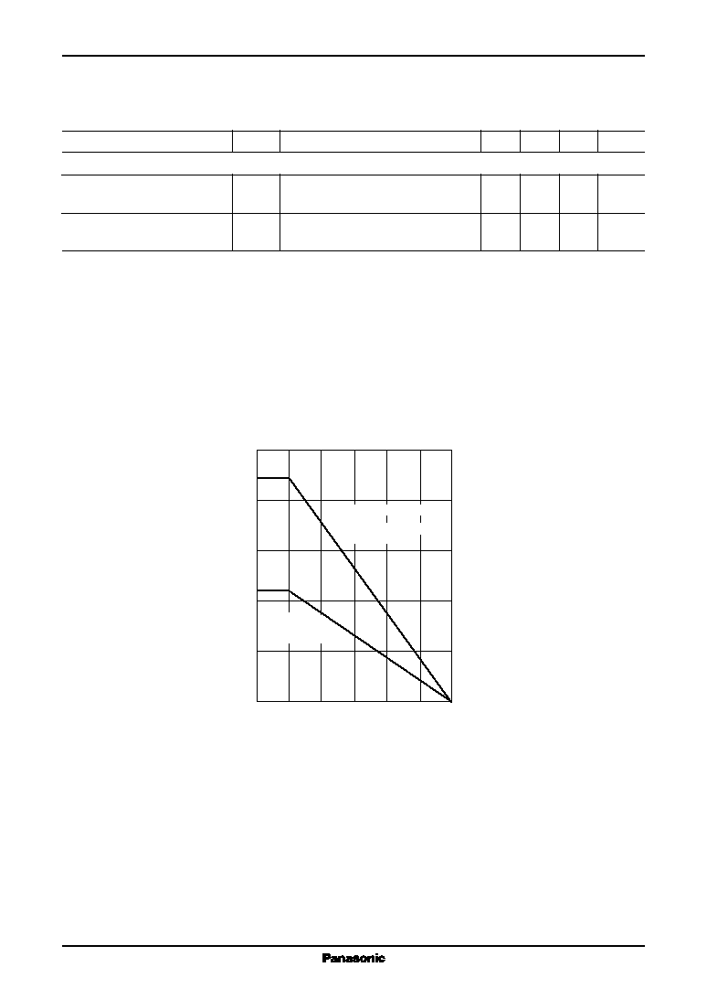
·
P
D
T
a
curves of HSOP042-P-0400
P
D
T
a
0.000
0
25
50
75
100
125
150
2.500
1.500
1.000
2.240
2.000
1.042
0.500
Ambient temperature T
a
(
°
C)
Po
wer dissipation
P
D
(W)
Mounted on standard board
(glass epoxy:
75 mm
×
75 mm
×
t1.6 mm)
R
th(j-a)
=
55.8
°
C/W
Independent IC
without a heat sink
R
th(j-a)
=
119.9
°
C/W
ICs for Compact Disc/CD-ROM Player
AN8814SB
5
s
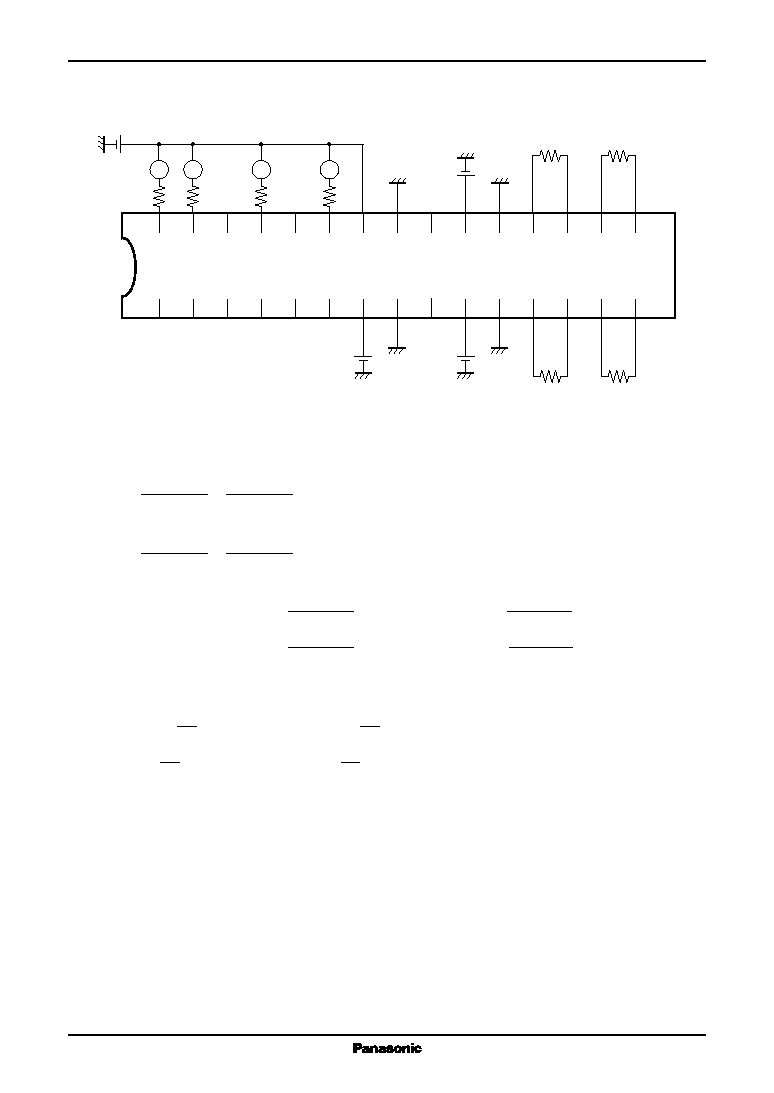
Application Circuit Example
1
28
R4
V
REF
RL1
2
27
3
26
4
25
5
24
6
23
7
SV
CC
22
Fin
Fin
8
21
9
20
10
19
11
18
12
17
13
16
14
15
V
4
R3
V
3
R2
V
2
R1
V
1
RL2
RL4
RL3
PV
CC1
PV
CC2
When the AN8814SB is use, take into account the following cautions and follow the power dissipation characteristic curve.
1. Load current I
P1
flowing into load RL1, RL2 is supplied through pin 20.
I
P1
=
|
V
18
-
V
17
|
+
|
V
16
-
V
15
|
R
L1
R
L2
2. Load current I
P2
flowing into load RL3, RL4 is supplied through pin 9.
I
P2
=
|
V
14
-
V
13
|
+
|
V
12
-
V
11
|
R
L3
R
L4
3. Dissipation increase (
P
D
) inside the IC (power output stage) caused by loads RL1, RL2, RL3 and RL4 is as follows:
P
D
=
(PV
CC1
-
|
V
18
-
V
17
|
)
× |
V
18
-
V
17
| +
(
PV
CC1
-
|
V
16
-
V
15
|
)
+ |
V
16
-
V
15
|
R
L1
R
L2
=
(PV
CC2
-
|
V
14
-
V
13
|
)
× |
V
14
-
V
13
| +
(
PV
CC2
-
|
V
12
-
V
11
|
)
× |
V
12
-
V
11
|
R
L3
R
L4
4. Dissipation increase (
P
S
) inside the IC (signal block supplied from pin 7) caused by loads RL1, RL2, RL3 and RL4
comes roughly as follows:
P
S
=
3
× {
V
1
×
(2
×
SV
CC
+
|
V
18
-
V
17
|
) +
V
2
×
(2
×
SV
CC
+
|
V
16
-
V
15
|
)
R
1
R
2
+
V
3
×
(2
×
SV
CC
+
|
V
14
-
V
13
|
) +
V
4
×
(2
×
SV
CC
+
|
V
12
-
V
11
|
)}
R
3
R
4
5. Dissipation increase in a driver operating mode is
P
D
+
P
S
.
6. Allowable power dissipation without load (P
D1
) can be found as follows:
P
D1
=
SV
CC
×
I
SVCC
+
PV
CC1
×
I
PVCC1
+
PV
CC2
×
I
PVCC2
7. Allowable power dissipation in a load operating mode (P
D
) comes roughly as follows:
P
D
=
P
D1
+
P
D
+
P
S