 | –≠–ª–µ–∫—Ç—Ä–æ–Ω–Ω—ã–π –∫–æ–º–ø–æ–Ω–µ–Ω—Ç: AN8816 | –°–∫–∞—á–∞—Ç—å:  PDF PDF  ZIP ZIP |
ICs for CD/CD-ROM Player
s
Overview
The AN8816SB is a 4ch. driver using the power opera-
tional amplifier method. It employs the surface mounting
type package superior in radiation characteristics.
s
Features
∑
Wide output D-range is available regardless of refer-
ence voltage on the system
∑
Setting of driver input/output gain enabled by external
resistance
∑
2ch. independently controllable PC (Power Cut) feature
built-in
∑
Thermal shut down circuit (with hysteresis) built-in
∑
Proper heat of IC controllable by separating the output
supply and setting each independently for 2ch.
∑
Construction of 5V supply enabled by external PNP Tr
∑
Accessary operational amplifier built-in
∑
Relatively easy pattern design by separating and con-
centrating the input line and output line
s
Application
Actuator for CD/CD-ROM, motor driver
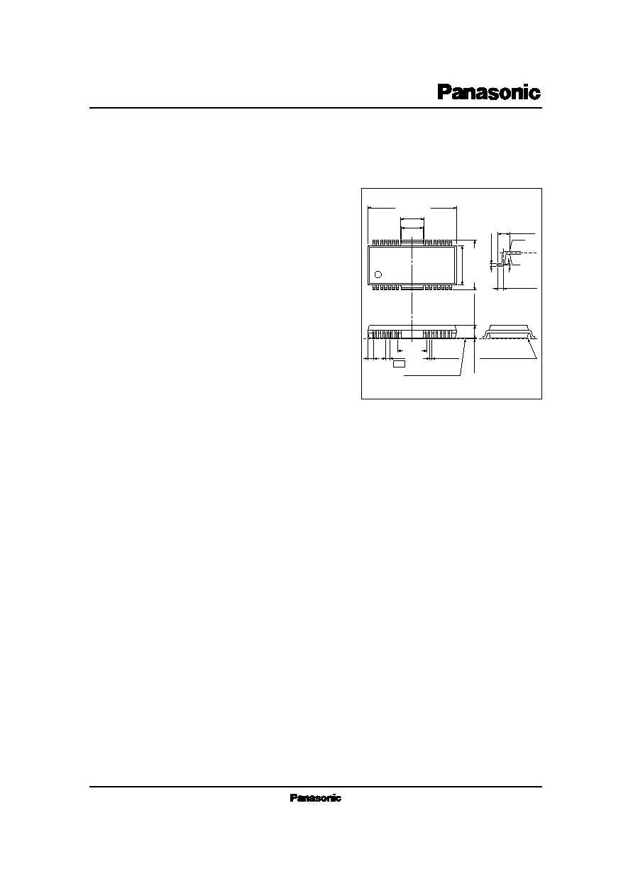
AN8816SB
4ch. Linear Driver IC for CD/CD-ROM
1
14
18.40
±
0.20
(5.15)
(4.80)
10.93
±
0.30
8.30
±
0.20
(6.40)
(1.20)
0.8
0.35
2.70
±
0.20
0.65
±
0.20
0 ~10∞
Unit : mm
7
8
28
15
22
21
(1.315)
0.30
+ 0.10
≠ 0.05
+0.10
≠ 0.05
0.10
±
0.10
SEATING PLANE
SEATING PLANE
Fin-attached 28-lead SOP package (HSOP-042-0400)
ICs for CD/CD-ROM Player
AN8816SB
s
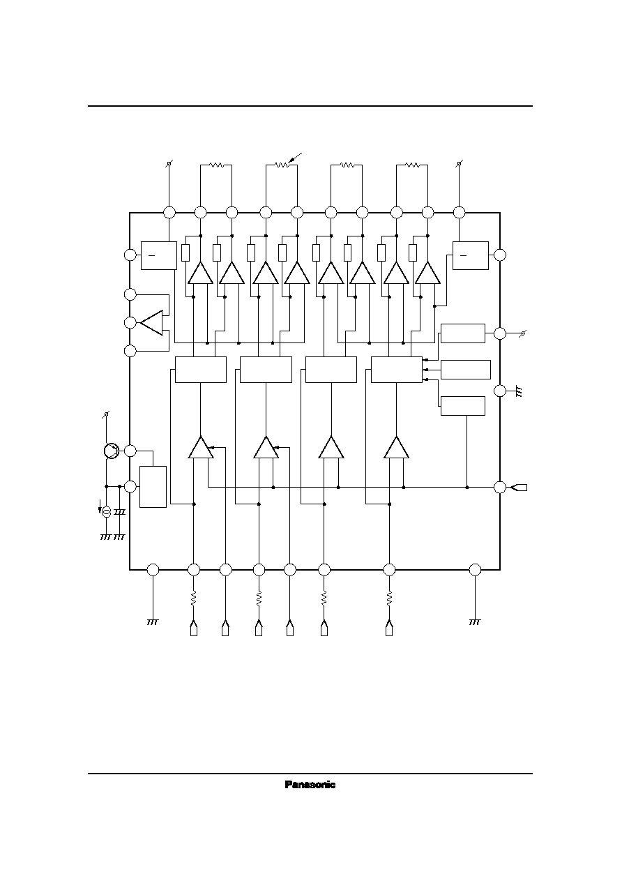
Block Diagram
23
25
27
19
9
11
12
13
14
15
16
17
18
20
7
Fin
22
2
1
5
6
4
21
PGND1
IN1
IN2
IN3
IN4
SV
CC
PV
CC1
VO1+
VO1≠
VO2+
VO2≠
VO3+
VO3≠
VO4+
VO4≠
PV
CC2
R
L4
R
L3
R
L2
R
L1
PV
CC
1
2
SV
CC
8
SGND
V
REF
+
≠
I
L
PV
CC
1
2
≠
+
24
26
28
10
PGND2
PC1
PC2
5V
reg
Motor or Coil
Direction
Det.
Direction
Det.
Direction
Det.
Direction
Det.
Thermal
Protector
V
CC
Monitor
V
REF
Monitor
≠ +
≠ +
≠ +
≠ +
≠ +
≠ +
≠ +
≠ +
≠ +
≠ +
≠ +
≠ +
ICs for CD/CD-ROM Player
AN8816SB
s
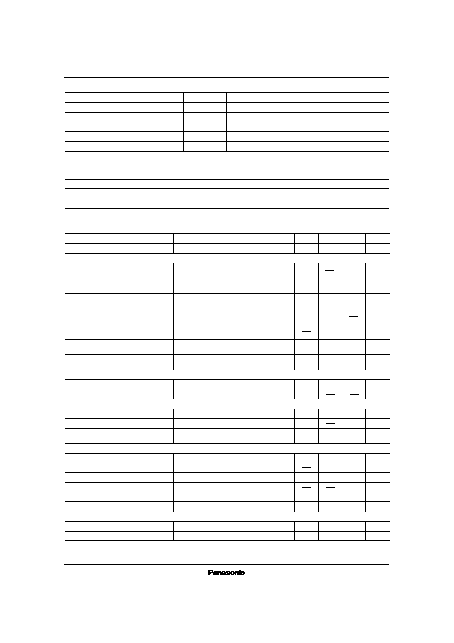
Absolute Maximum Ratings
(Ta=25∞C)
V
CC
I
CC
P
D
T
opr
T
stg
Supply Voltage
Supply Current
Power Dissipation
Note)
Operating Ambient Temperature
Storage Temperature
V
mA
mW
∞C
∞C
Parameter
Symbol
Rating
Unit
18
3141
≠30 ~ + 85
≠55 ~ + 150
Note) For surface mounting on 100
◊
80
◊
1.6 mm double face glass epoxy board.
s
Recommended Operating Range
(Ta=25∞C)
5.5V ~ 14V
Parameter
Symbol
Range
Operating Supply Voltage Range
SV
CC
Note)
PV
CC1
, PV
CC2
Note) Set SV
CC
to the maximum electric potential.
s
Electrical Characteristics
(Ta=25∞C)
Parameter
Symbol
Condition
min.
typ.
max.
Unit
Drivers 1 to 4
Input Offset Voltage
Output Offset Voltage
Gain
Maximum Output Amplitude (+)
Maximum Output Amplitude (≠)
Threshold H
Threshold L
V
IOF
V
OOF
G
V
L+
V
L≠
V
PCH
V
PCL
mV
mV
dB
V
V
V
V
5
≠50
15
5
500
1.7
( )
( )
20
5.0
≠5.0
Total Circuit Current
I
tot
PV
CC1
= PV
CC2
= SV
CC
= 8V
PV
CC1
= PV
CC2
= SV
CC
= 8V
R
L
= 8
, R
IN
= 10k
3.0
2.0
10
mA
3.3
≠10
≠50
18
4.4
2.0
10
50
22
≠4.4
0.3
Reset Circuit
Reset Operation Release Supply Voltage
V
REF
Detection
5V Regulator
Output Voltage
Output Load Fluctuation
Supply Voltage Fluctuation
V
RST
V
REF
3.2
V
V
I
IN
= 10
µ
A, R
IN
= 10k
4.75
5.25
50
5
V
REG
DV
R
DV
V
5.0
V
mV
mV
PV
CC1
= PV
CC2
= SV
CC
= 8V
PV
CC1
= PV
CC2
= SV
CC
= 8V
PV
CC1
= PV
CC2
= SV
CC
= 8V~12V
≠5
100
≠5
6.0
2.0
2.0
( )
( )
mV
nA
V
V
mA
mA
OP Amp.
Input Offset Voltage
Input Bias Current
High Level Output Voltage
Low Level Output Voltage
Output Drive Current Sink
Output Drive Current Source
V
OF
I
BOP
V
OH
V
OL
I
SIN
I
SOU
PV
CC1
= PV
CC2
= SV
CC
= 8V
PV
CC1
= PV
CC2
= SV
CC
= 8V
PV
CC1
= PV
CC2
= SV
CC
= 8V
PV
CC1
= PV
CC2
= SV
CC
= 8V
PV
CC1
= PV
CC2
= SV
CC
= 8V
PV
CC1
= PV
CC2
= SV
CC
= 8V
Heat Protection Circuit
Operation Temperature Equilibrium Value
Note 1)
Operation Temperature Hysteresis Width
Note 1)
T
THD
DT
THD
(180)
(45)
∞C
∞C
PV
CC1
= PV
CC2
= SV
CC
= 8V
R
L
= 8
, R
IN
= 10k
PV
CC1
= PV
CC2
= SV
CC
= 8V
R
L
= 8
, R
IN
= 10k
PV
CC1
= PV
CC2
= SV
CC
= 8V
R
L
= 8
, R
IN
= 10k
PV
CC1
= PV
CC2
= SV
CC
= 8V
R
L
= 8
, R
IN
= 10k
PV
CC1
= PV
CC2
= SV
CC
= 8V
R
L
= 8
, R
IN
= 10k
PV
CC1
= PV
CC2
= SV
CC
= 8V
R
L
= 8
, R
IN
= 10k
Note 1) Characteristic value in parentheses is a reference value for design but not a guaranteed value.
ICs for CD/CD-ROM Player
AN8816SB
s
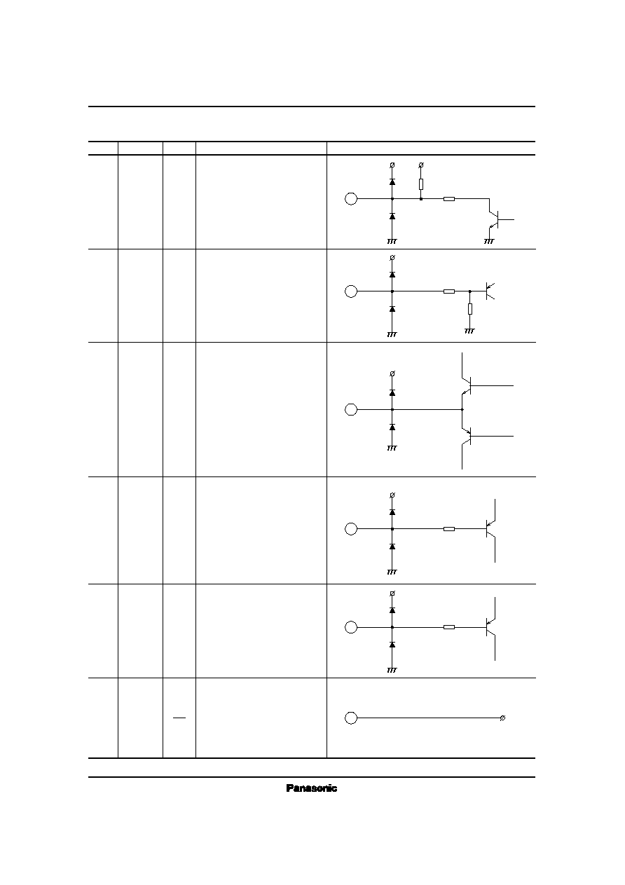
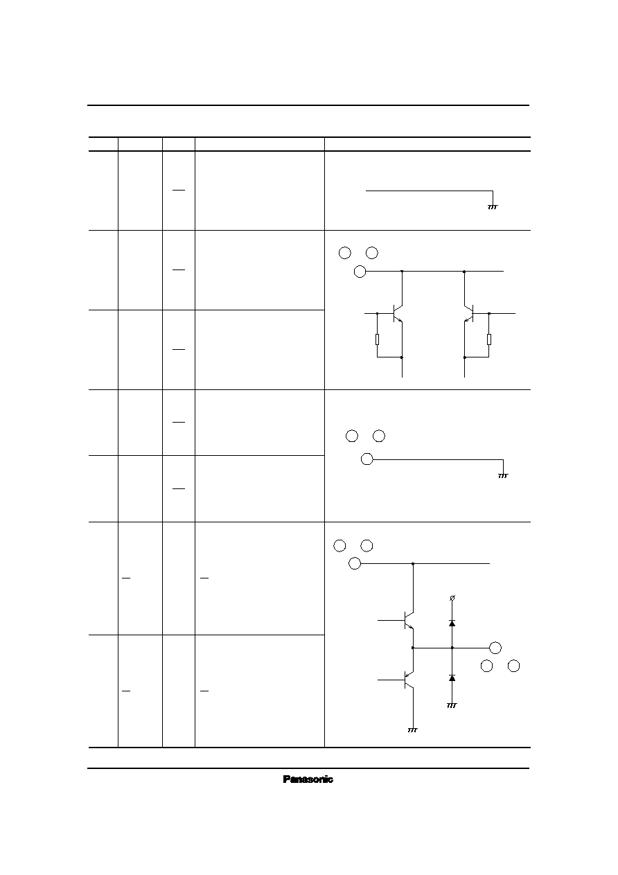
Pin Description
Pin Description
Equivalent Circuit
Pin No.
1
2
Symbol
I/O
4
5
6
7
TB
V
MON
OPO
IN≠
IN+
SV
CC
O
I
O
I
I
Output pin for controlling the
power transistor base of 5V
Monitor input pin for 5V regulator
output
Output pin of op-amp.
Inverting input pin of op-amp.
SV
CC
pin for driver control circuit,
not connected with power V
CC
pin
Non-inverting input pin of op-amp.
1
2
4
5
6
7
ICs for CD/CD-ROM Player
AN8816SB
s
Pin Description (Cont.)
Pin Description
Equivalent Circuit
Pin No.
Fin
20
Symbol
I/O
SGND pin for driver control
circuit
Power V
CC
pin supplying the
current flowing in output power
transistors, 15, 16, 17, and 18
9
19
10
21
8
SGND
PV
CC
1
PV
CC
2
PGND1
PGND2
PV
CC
1
PV
CC
2
1
2
1
2
O
O
Power V
CC
pin supplying the
current flowing in output power
transistors, 11, 12, 13, and 14
GND pin for output transistors 15,
16, 17, and 18
GND pin for output transistors 11,
12, 13, and 14
PV
CC
output pin 1
PV
CC
output pin 2
1
2
1
2
Fin
20
or
9
19
or
10
20
or
9
21
or
8
SV
CC
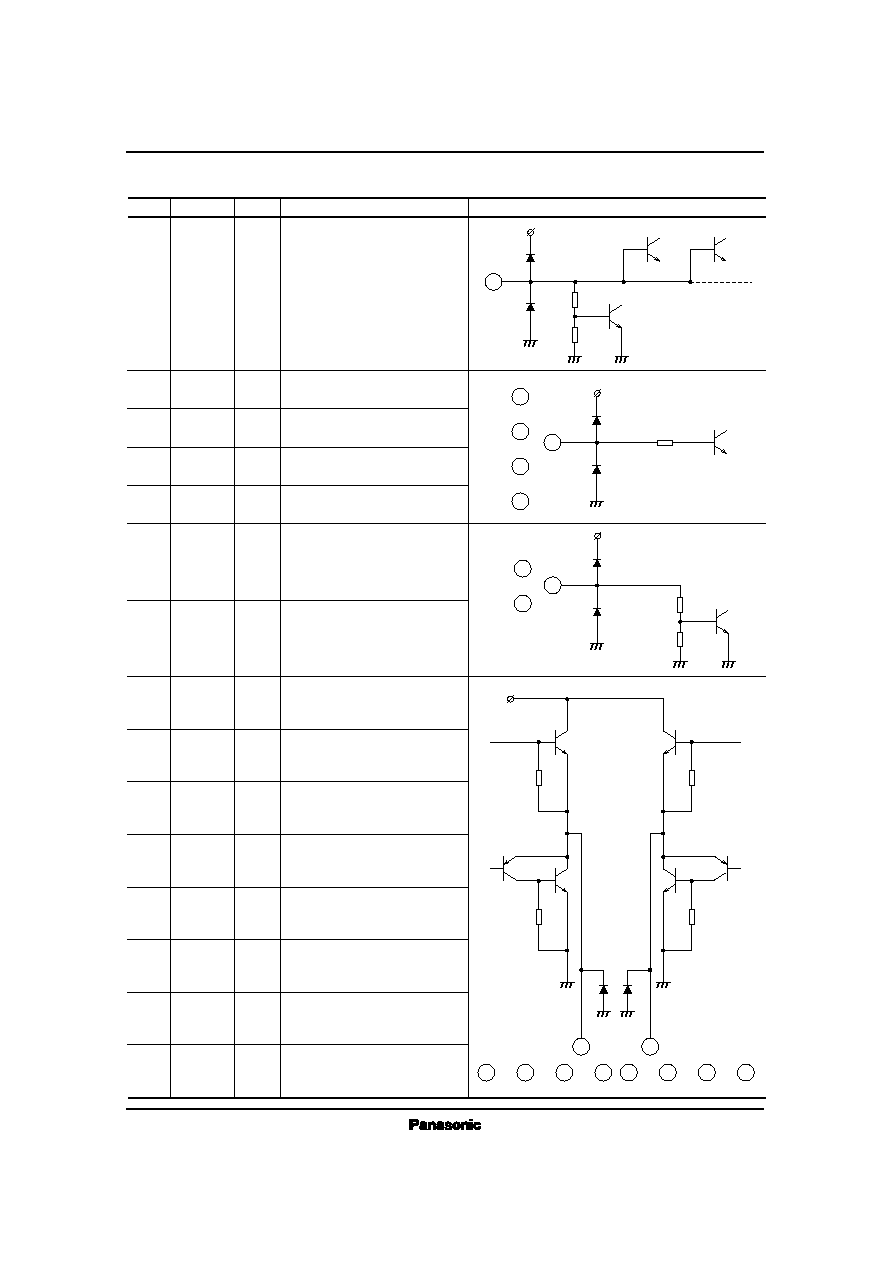
ICs for CD/CD-ROM Player
AN8816SB
s
Pin Description (Cont.)
Pin Description
Equivalent Circuit
Pin No.
22
Symbol
I/O
23
25
27
28
24
26
11
12
13
14
15
16
17
18
V
REF
PC1
PC2
VO4≠
VO4+
VO3≠
VO3+
VO2≠
VO2+
VO1≠
VO1+
I
I
I
I
I
I
I
O
O
O
O
O
O
O
O
V
REF
input pin
Input pin of Driver 1
Input pin of Driver 2
Input pin of Driver 3
Input pin of Driver 4
Power cut input pin of Driver 1
Reverse rotation output pin of Driver 4
Normal rotation output pin of Driver 4
Reverse rotation output pin of Driver 3
Normal rotation output pin of Driver 3
Reverse rotation output pin of Driver 2
Normal rotation output pin of Driver 2
Reverse rotation output pin of driver 1
Normal rotation output pin of Driver 1
IN1
IN2
IN3
IN4
Power cut input pin of Driver 2
23
25
24
26
27
SV
CC
SV
CC
PV
CC
or
or
12
or
14
or
16
or
18
11
or
13
or
15
or
17
or
28
or
22
SV
CC
14k
30k
ICs for CD/CD-ROM Player
AN8816SB
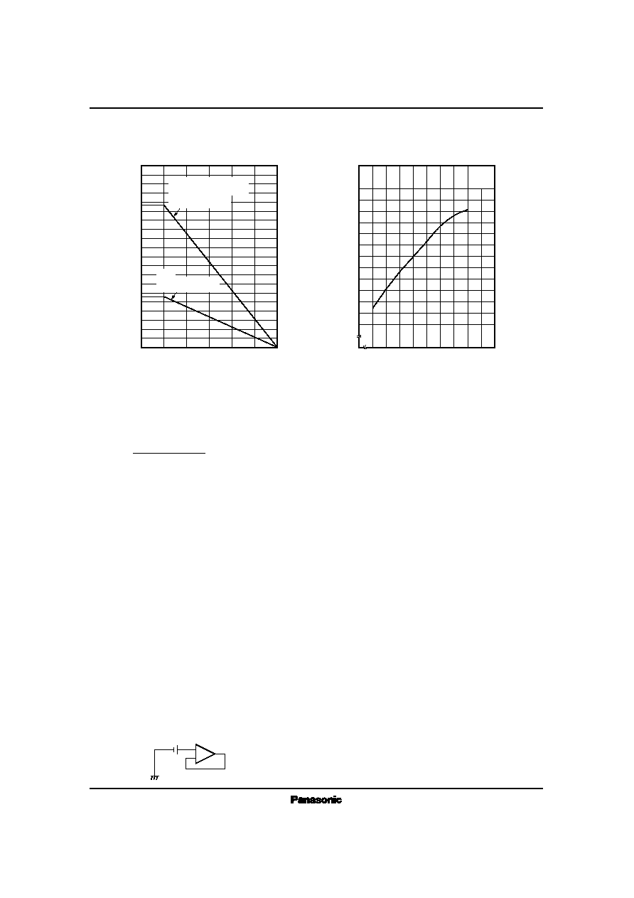
s
Characteristic Curve
8.0
7.0
6.0
5.0
4.0
3.0
2.0
V
CC
(V)
O
u
t
p
u
t
D
-
R
a
n
g
e
(
V
)
6
5
9
12
11
7
8
10
13
R
L
= 8
4,000
3,600
3,200
2,800
2,400
2,000
1,600
1,200
800
400
0
Ambient Temperature Ta (∞C)
P
o
w
e
r
D
i
s
s
i
p
a
t
i
o
n
P
D
(
m
W
)
25
0
75
125
50
100
150
Glass epoxy board
(100mm
◊
80mm
◊
1.6mm)
Rthj≠ a = 39.8∞C/W
P
D
= 3141mW (25∞C)
Unit
Rthj≠ a = 111.6∞C/W
P
D
= 1120mW (25∞C)
3,141
1,120
V
CC
≠ Maximum Output Amplitude Characteristics
P
D
≠Ta
≠
+
V
REF
s
Description for use
∑ Driver Portion
Calculate the driver gain by using the following formula for setting.
G =
60k
◊
2
R
IN1
+100 (
)
The power supply for Ch.1 and 2 is supplied from Pin20 and the power supply for Ch.3 and 4 is supplied from Pin9
independently.
Output amplitude is increased by increasing the supply voltage. Set the power supply voltage as necessary. However, always set
Pin7 of V
CC
to the maximum electric potential.
Pin8 and 21 may require a capacitor for ripple removal.
As protection functions, V
CC
reset circuit,V
REF
detector and heat protection circuit are incorporated.
The V
CC
reset circuit operates at approx. 3V and is released at 3.2V, when the supply (Pin7) decreases. For the V
REF
detector, the
protection function works at approx. 1V (max. 2V).
Also, the set temperature for operation of the heat protection circuit is approx. 180∞C .
PC (Power Cut) functions which can be independently controlled are incorporated in Ch.1 and 2.
∑ 5V Supply
By adding an external PNP transistor, 5V regulator can be constructed. Attach an external capacitor for loop filter to output Pin2.
In Pin1, the base current limiting circuit (typ. 10mA) is incorporated.
When the V supply is used, the external PNP Tr emitter must be connected to pin than Pin7 (SV
CC
pin)
∑ OP Amp.
When the operational amplifier is not used, make connection as follows ;
ICs for CD/CD-ROM Player
AN8816SB
24
23
22
21
20
19
18
17
16
15
1
2
3
4
5
6
7
8
9
10
11
12
13
14
AN8816SB
s
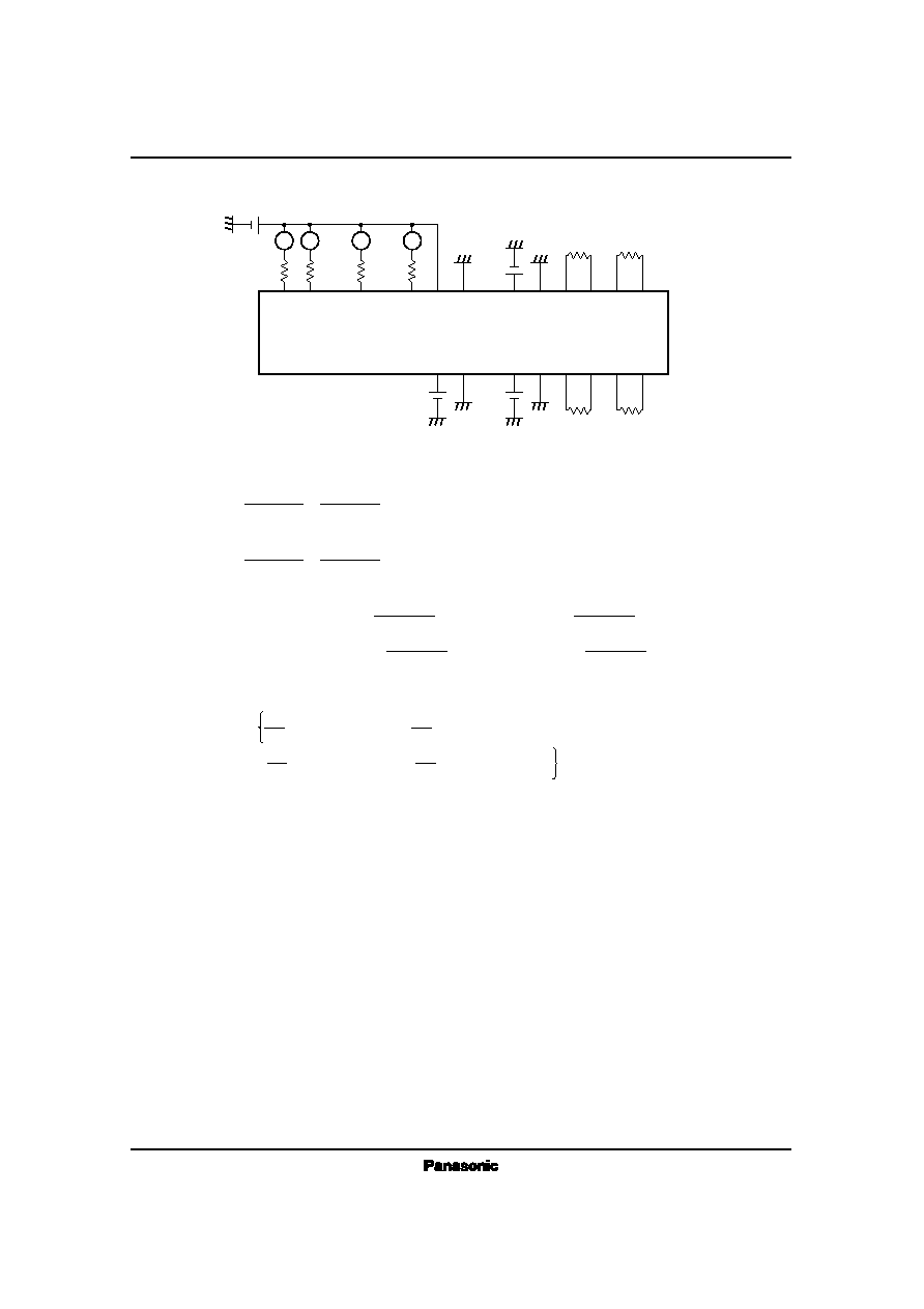
Cautions for use
When the AN8816SB is used, take into account the following cautions and follow the power dissipation characteristic curve.
(1) Load current, I
P1
flowing in loads R
L1
and R
L2
is supplied through Pin20.
(2) Load current, I
P2
flowing in loads R
L3
and R
L4
is supplied through Pin9.
(3) Dissipation increase (DP
d
) inside the IC (power output stage) caused by loads R
L1
, R
L2
, R
L3
, R
L4
is as follow.
(4) Dissipation increase (DP
S
) inside the IC (signal block supplied from Pinu) caused by loads R
L1
, R
L2
, R
L3
, R
L4
is almost as
follows ;
(5) Dissipation increase during driver running is DP
d
+ DP
S
.
(6) Inside loss under no load (P
d1
) is almost as follows ;
(7) Entire IC inside loss (P
d
) is almost as follows ;
PV
CC1
R
L4
R
L3
R
L2
SV
CC
PV
CC2
I
P1
=
|
V
18
≠V
17
|
R
L1
+
|
V
16
≠V
15
|
R
L2
I
P2
=
|
V
14
≠V
13
|
R
L3
+
|
V
12
≠V
11
|
R
L4
P
d1
= SV
CC
◊
I (SV
CC
)
+ PV
CC1
◊
I (PV
CC1
)
+ PV
CC2
◊
I (PV
CC2
)
P
d
= P
d1
+ DP
d
+ DP
S
DP
d
= (PV
CC1
≠ |
V
18
≠V
17
|
)
◊
|
V
18
≠V
17
|
R
L1
+ (PV
CC1
≠ |
V
16
≠V
15
|
)
◊
|
V
16
≠V
15
|
R
L2
+ (PV
CC2
≠ |
V
14
≠V
13
|
)
◊
|
V
14
≠V
13
|
R
L3
+ (PV
CC2
≠ |
V
12
≠V
11
|
)
◊
|
V
12
≠V
11
|
R
L4
28
26
25
27
R
L1
+
DP
S
= 3
V
1
R
1
(2SV
CC
+ |
V
18
≠V
17
|
)
+
V
2
R
2
(2SV
CC
+ |
V
16
≠V
15
|
)
V
3
R
3
(2SV
CC
+ |
V
14
≠V
13
|
)
+
(2SV
CC
+ |
V
12
≠V
11
|
)
V
4
R
4
Fin
Fin
V
2
V
3
R
2
R
3
V
REF
V
4
R
4
V
1
R
1