1
Power Transistors
2SB1148, 2SB1148A
Silicon PNP epitaxial planar type
For low-voltage switching
Complementary to 2SD1752 and 2SD1752A
s
Features
q
Low collector to emitter saturation voltage V
CE(sat)
q
High-speed switching
q
I type package enabling direct soldering of the radiating fin to
the printed circuit board, etc. of small electronic equipment.
s
Absolute Maximum Ratings
(T
C
=25∞C)
Parameter
Collector to
base voltage
Collector to
emitter voltage
Emitter to base voltage
Peak collector current
Collector current
Collector power
dissipation
Junction temperature
Storage temperature
Symbol
V
CBO
V
CEO
V
EBO
I
CP
I
C
P
C
T
j
T
stg
Ratings
≠40
≠50
≠20
≠40
≠7
≠20
≠10
15
1.3
150
≠55 to +150
Unit
V
V
V
A
A
W
∞C
∞C
2SB1148
2SB1148A
2SB1148
2SB1148A
T
C
=25
∞
C
Ta=25
∞
C
s
Electrical Characteristics
(T
C
=25∞C)
Parameter
Collector cutoff
current
Emitter cutoff current
Collector to emitter
voltage
Forward current transfer ratio
Collector to emitter saturation voltage
Base to emitter saturation voltage
Transition frequency
Collector output capacitance
Turn-on time
Storage time
Fall time
Symbol
I
CBO
I
EBO
V
CEO
h
FE1
h
FE2
*
V
CE(sat)
V
BE(sat)
f
T
C
ob
t
on
t
stg
t
f
Conditions
V
CB
= ≠40V, I
E
= 0
V
CB
= ≠50V, I
E
= 0
V
EB
= ≠5V, I
C
= 0
I
C
= ≠10mA, I
B
= 0
V
CE
= ≠2V, I
C
= ≠ 0.1A
V
CE
= ≠2V, I
C
= ≠3A
I
C
= ≠10A, I
B
= ≠ 0.33A
I
C
= ≠10A, I
B
= ≠ 0.33A
V
CE
= ≠10V, I
C
= ≠ 0.5A, f = 10MHz
V
CB
= ≠10V, I
E
= 0, f = 1MHz
I
C
= ≠3A, I
B1
= ≠ 0.1A, I
B2
= 0.1A,
V
CC
= ≠20V
min
≠20
≠40
45
90
typ
100
400
0.1
0.5
0.1
max
≠50
≠50
≠50
260
≠ 0.6
≠1.5
Unit
µ
A
µ
A
V
V
V
MHz
pF
µ
s
µ
s
µ
s
2SB1148
2SB1148A
2SB1148
2SB1148A
*
h
FE2
Rank classification
Rank
Q
P
h
FE2
90 to 180
130 to 260
Unit: mm
1:Base
2:Collector
3:Emitter
I Type Package
Unit: mm
1:Base
2:Collector
3:Emitter
I Type Package (Y)
7.2
±
0.3
7.0
±
0.3
3.0
±
0.2
3.5
±
0.2
10.0
+0.3
≠0.
0.8
±
0.2
1.0
±
0.2
4.6
±
0.4
2
1
3
1.1
±
0.1
0.75
±
0.1
2.3
±
0.2
0.85
±
0.1
0.4
±
0.1
7.0
±
0.3
0.75
±
0.1
2.3
±
0.2
4.6
±
0.4
1.1
±
0.1
10.2
±
0.3
7.2
±
0.3
2.0
±
0.2
0.9
±
0.1
3.5
±
0.2
2.5
±
0.2
1.0
1.0
2.5
±
0.2
3.0
±
0.2
1.0 max.
1
2
3
0 to 0.15
0 to 0.15
2.5
0.5 max.
2
Power Transistors
2SB1148, 2SB1148A
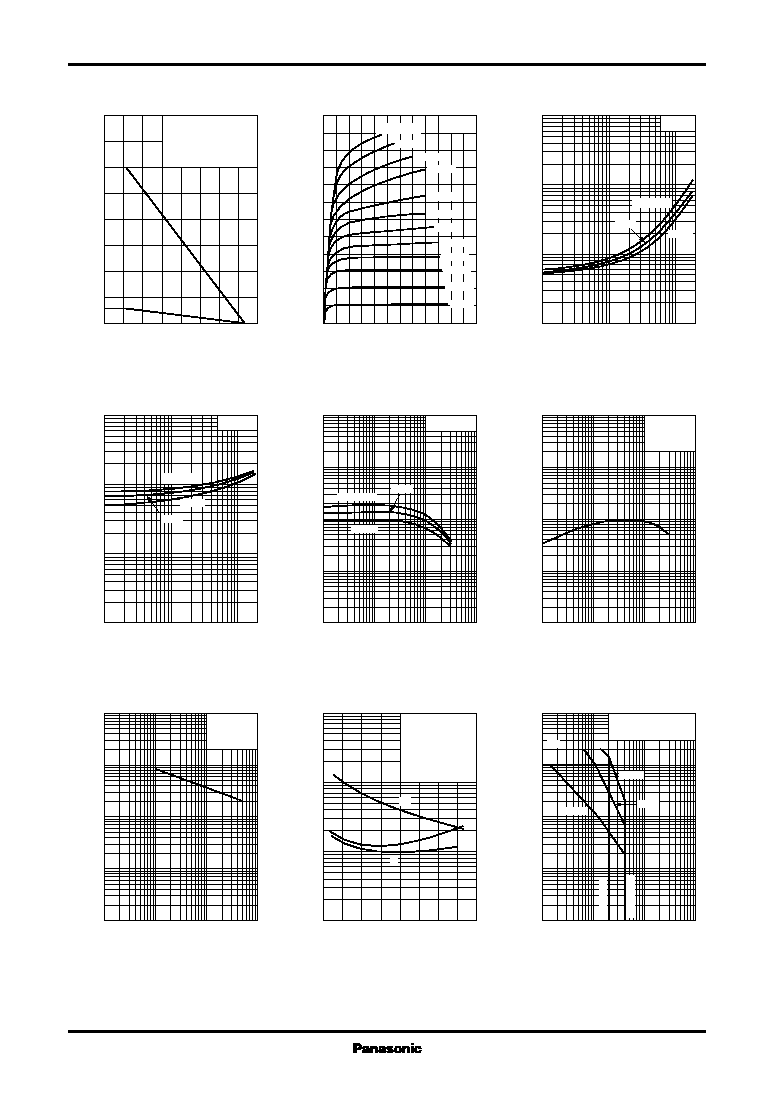
P
C
-- Ta
I
C
-- V
CE
V
CE(sat)
-- I
C
V
BE(sat)
-- I
C
h
FE
-- I
C
f
T
-- I
C
C
ob
-- V
CB
t
on
, t
stg
, t
f
-- I
C
Area of safe operation (ASO)
0
160
40
120
80
140
20
100
60
0
20
15
5
10
(1) T
C
=Ta
(2) Without heat sink
(P
C
=1.3W)
(1)
(2)
Ambient temperature Ta (∞C)
Collector power dissipation P
C
(W
)
0
≠12
≠10
≠8
≠2
≠6
≠4
0
≠12
≠10
≠8
≠6
≠4
≠2
T
C
=25∞C
≠80mA
≠60mA
≠50mA
≠40mA
≠35mA
≠20mA
≠15mA
≠30mA
≠25mA
≠10mA
≠5mA
I
B
=≠100mA
Collector to emitter voltage V
CE
(V)
Collector current I
C
(A
)
≠ 0.1
≠1
≠10
≠ 0.3
≠3
≠ 0.01
≠10
≠1
≠ 0.1
≠ 0.03
≠ 0.3
≠3
I
C
/I
B
=30
T
C
=100∞C
≠25∞C
25∞C
Collector current I
C
(A)
Collector to emitter saturation voltage V
CE(sat)
(V
)
≠ 0.1
≠1
≠10
≠ 0.3
≠3
≠ 0.01
≠10
≠1
≠ 0.1
≠ 0.03
≠ 0.3
≠3
I
C
/I
B
=30
T
C
=≠25∞C
25∞C
100∞C
Collector current I
C
(A)
Base to emitter saturation voltage V
BE(sat)
(V
)
≠ 0.1
≠1
≠10
≠100
≠ 0.3
≠3
≠30
1
3
10
30
100
300
1000
3000
10000
V
CE
=≠2V
T
C
=100∞C
25∞C
≠25∞C
Collector current I
C
(A)
Forward current transfer ratio h
FE
≠ 0.01
≠ 0.1
≠1
≠10
≠ 0.03
≠ 0.3
≠3
1
3
10
30
100
300
1000
3000
10000
V
CE
=≠10V
f=10MHz
T
C
=25∞C
Collector current I
C
(A)
Transition frequency f
T
(MHz
)
≠ 0.1
≠1
≠10
≠100
≠ 0.3
≠3
≠30
1
3
10
30
100
300
1000
3000
10000
I
E
=0
f=1MHz
Ta=25∞C
Collector to base voltage V
CB
(V)
Collector output capacitance C
ob
(pF
)
0
≠8
≠2
≠6
≠4
≠7
≠1
≠5
≠3
0.01
10
1
0.1
0.03
0.3
3
t
stg
t
on
t
f
Pulsed t
w
=1ms
Duty cycle=1%
I
C
/I
B
=30
(≠I
B1
=I
B2
)
V
CC
=≠20V
T
C
=25∞C
Collector current I
C
(A)
Switching time t
on
,t
stg
,t
f
(
µ
s
)
≠1
≠10
≠100
≠1000
≠3
≠30
≠300
≠ 0.01
≠ 0.03
≠ 0.1
≠ 0.3
≠1
≠3
≠10
≠30
≠100
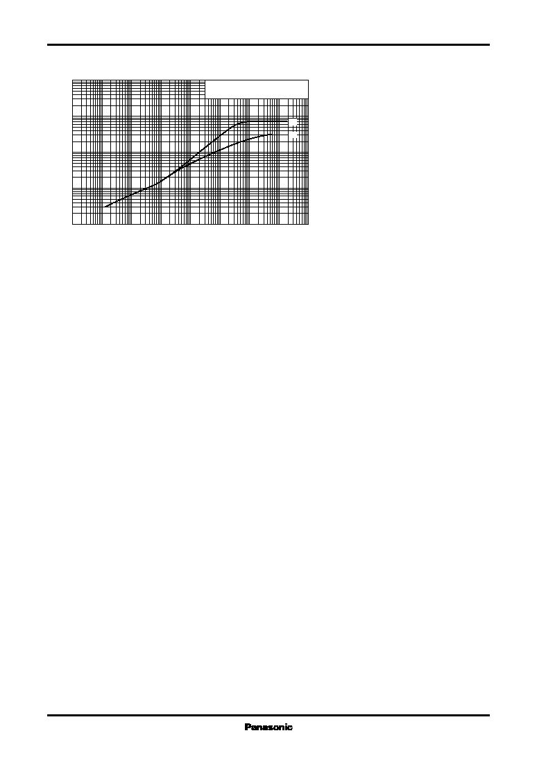
Non repetitive pulse
T
C
=25∞C
10ms
300ms
t=1ms
I
CP
I
C
2SB1148A
2SB1148
Collector to emitter voltage V
CE
(V)
Collector current I
C
(A
)