1
Power Transistors
2SC4111
Silicon NPN triple diffusion planar type
For horizontal deflection output
s
Features
q
High-speed switching
q
High collector to base voltage V
CBO
q
Wide area of safe operation (ASO)
q
Satisfactory linearity of foward current transfer ratio h
FE
s
Absolute Maximum Ratings
(T
C
=25∞C)
Parameter
Collector to base voltage
Collector to emitter voltage
Emitter to base voltage
Peak collector current
Collector current
Base current
Collector power
dissipation
Junction temperature
Storage temperature
Symbol
V
CBO
V
CES
V
CEO
V
EBO
I
CP
I
C
I
B
P
C
T
j
T
stg
Ratings
1500
1500
700
7
22
10
3.5
150
3.5
150
≠55 to +150
Unit
V
V
V
V
A
A
A
W
∞C
∞C
T
C
=25
∞
C
Ta=25
∞
C
s
Electrical Characteristics
(T
C
=25∞C)
Parameter
Collector cutoff current
Emitter to base voltage
Forward current transfer ratio
Collector to emitter saturation voltage
Base to emitter saturation voltage
Transition frequency
Storage time
Fall time
Symbol
I
CBO
V
EBO
h
FE1
h
FE2
V
CE(sat)
V
BE(sat)
f
T
t
stg
t
f
Conditions
V
CB
= 750V, I
E
= 0
V
CB
= 1500V, I
E
= 0
I
C
= 1mA, I
B
= 0
V
CE
= 5V, I
C
= 1A
V
CE
= 5V, I
C
= 7A
I
C
= 7A, I
B
= 2.5A
I
C
= 7A, I
B
= 2.5A
V
CE
= 10V, I
C
= 1A, f = 0.5MHz
I
C
= 6A, L
leak
= 5
µ
H,
I
B1
= 1.7A, I
B2
= ≠1.7A
min
7
5
3
typ
2
max
10
1
8
5
1.5
12
0.6
Unit
µ
A
mA
V
V
V
MHz
µ
s
µ
s
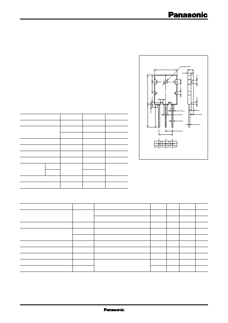
Unit: mm
1:Base
2:Collector
3:Emitter
TOP≠3L Package
20.0
±
0.5
6.0
10.0
26.0
±
0.5
20.0
±
0.5
1.5
2.5
Solder Dip
10.9
±
0.5
1
2
3
2.0
±
0.3
3.0
±
0.3
1.0
±
0.2
5.0
±
0.3
3.0
4.0
2.0
5.45
±
0.3
0.6
±
0.2
1.5
2.7
±
0.3
1.5
2.0
3.3
±
0.2
3.0
2
Power Transistors
2SC4111
P
C
-- Ta
I
C
-- V
CE
V
CE(sat)
-- I
C
V
BE(sat)
-- I
C
h
FE
-- I
C
f
T
-- I
C
C
ob
-- V
CB
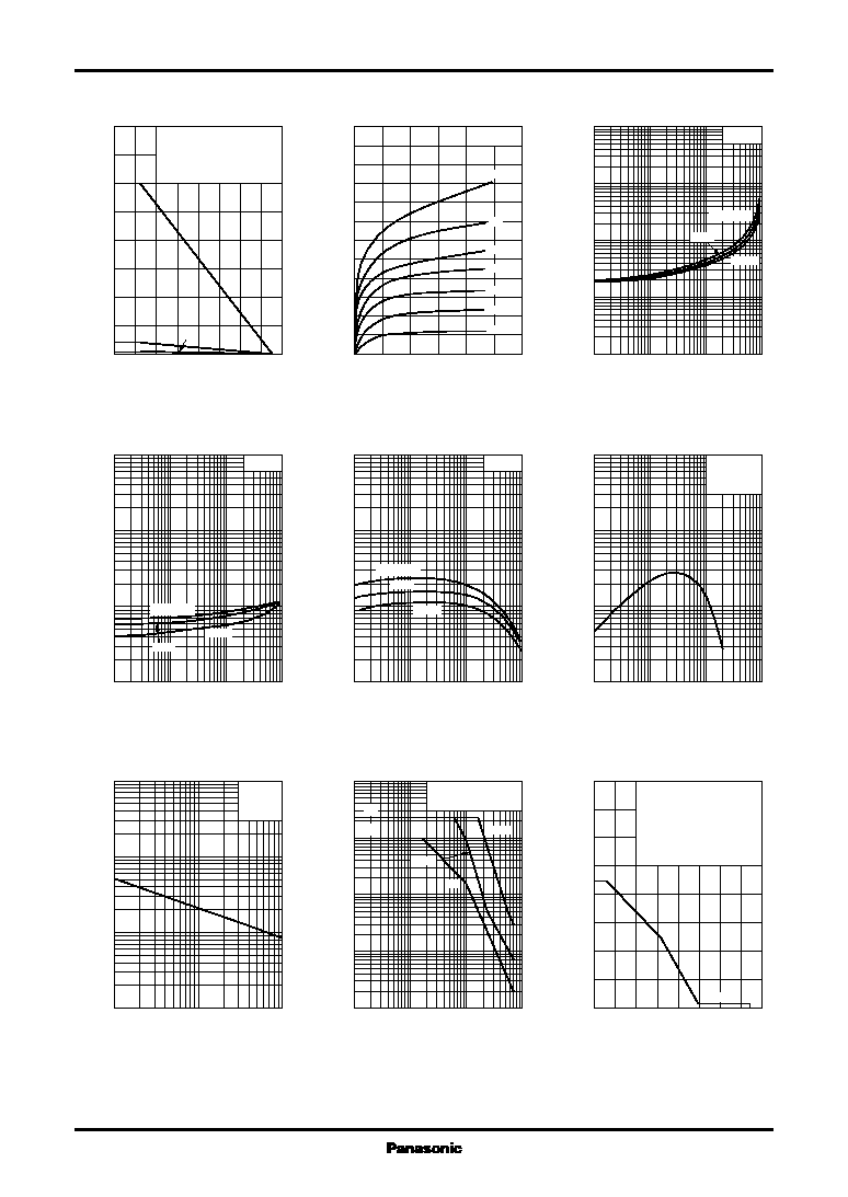
Area of safe operation (ASO)
Area of safe operation, horizontal operation ASO
0
160
40
120
80
140
20
100
60
0
200
150
50
100
(1)
(3)
(2)
(1) T
C
=Ta
(2) With a 100
◊
100
◊
2mm
Al heat sink
(3) With a 50
◊
50
◊
2mm
Al heat sink
Ambient temperature Ta (∞C)
Collector power dissipation P
C
(W
)
0
12
10
8
2
6
4
0
12
10
8
6
4
2
T
C
=25∞C
0.1A
0.05A
0.2A
0.5A
0.7A
1A
I
B
=2A
Collector to emitter voltage V
CE
(V)
Collector current I
C
(A
)
0.01
0.1
1
10
0.03
0.3
3
0.01
0.03
0.1
0.3
1
3
10
30
100
I
C
/I
B
=2.8
≠25∞C
25∞C
T
C
=100∞C
Collector current I
C
(A)
Collector to emitter saturation voltage V
CE(sat)
(V
)
0.01
0.1
1
10
0.03
0.3
3
0.1
100
10
1
0.3
3
30
I
C
/I
B
=2.8
T
C
=≠25∞C
25∞C
100∞C
Collector current I
C
(A)
Base to emitter saturation voltage V
BE(sat)
(V
)
0.01
0.1
1
10
0.03
0.3
3
1
1000
100
10
3
30
300
V
CE
=5V
T
C
=100∞C
≠25∞C
25∞C
Collector current I
C
(A)
Forward current transfer ratio h
FE
0.01
0.1
1
10
0.03
0.3
3
0.1
100
10
1
0.3
3
30
V
CE
=10V
f=0.5MHz
T
C
=25∞C
Collector current I
C
(A)
Transition frequency f
T
(MHz
)
1
3
10
30
100
10
10000
1000
100
30
300
3000
I
E
=0
f=1MHz
T
C
=25∞C
Collector to base voltage V
CB
(V)
Collector output capacitance C
ob
(pF
)
1
10
100
1000
3
30
300
0.01
0.03
0.1
0.3
1
3
10
30
100
Non repetitive pulse
T
C
=25∞C
I
CP
I
C
DC
10ms
t=1ms
Collector to emitter voltage V
CE
(V)
Collector current I
C
(A
)
0
1600
400
1200
800
1400
200
1000
600
0
40
30
10
25
35
20
5
15
I
CP
<1mA
f=15.75kHz, T
C
=25∞C
Area of safe operation for
the single pulse load curve
due to discharge in the
high-voltage rectifier tube
during horizontal operation
Collector to emitter voltage V
CE
(V)
Collector current I
C
(A
)
3
Power Transistors
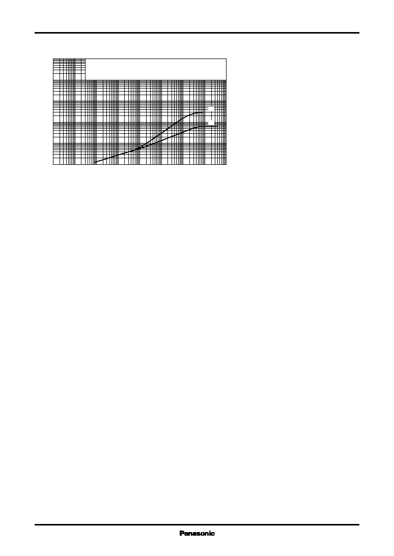
2SC4111
R
th(t)
-- t
10
≠4
10
10
≠3
10
≠1
10
≠2
1
10
3
10
2
10
4
0.1
1
10
100
10000
1000
Note: R
th
was measured at Ta=25∞C and under natural convection.
(1) P
T
=10V
◊
0.3A (3W) and without heat sink
(2) P
T
=10V
◊
1.0A (10W) and with a 100
◊
100
◊
2mm Al heat sink
(1)
(2)
Time t (s)
Thermal resistance R
th
(t)
(∞C/W
)