1SMB3EZ11 THRU 1SMB3EZ200
SURFACE MOUNT SILICON ZENER DIODE
VOLTAGE - 11 TO 200 Volts Power - 3.0 Watts
FEATURES
l
For surface mounted applications in order to
optimize board space
l
Low profile package
l
Built-in strain relief
l
Glass passivated junction
l
Low inductance
l
Excellent clamping capability
l
Typical I
D
less than 1
£g
A above 11V
l
High temperature soldering :
260
¢J
/10 seconds at terminals
l
Plastic package has Underwriters Laboratory
Flammability Classification 94V-O
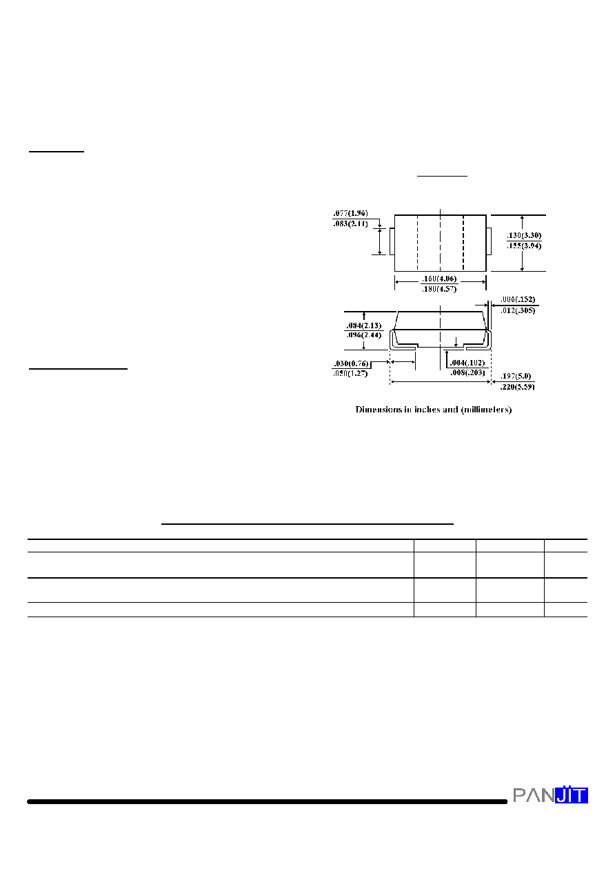
MECHANICAL DATA
Case: JEDEC DO-214AA, Molded plastic over
passivated junction
Terminals: Solder plated, solderable per
MIL-STD-750, method 2026
Polarity: Color band denotes positive end (cathode)
except Bidirectional
Standard Packaging: 12mm tape(EIA-481)
Weight: 0.003 ounce, 0.093 gram
MAXIMUM RATINGS AND ELECTRICAL CHARACTERISTICS
Ratings at 25
¢J
ambient temperature unless otherwise specified.
SYMBOL
VALUE
UNITS
Peak Pulse Power Dissipation (Note A)
Derate above 75
¢J
P
D
3
24
Watts
mW/
¢J
Peak forward Surge Current 8.3ms single half sine-wave superimposed on rated
load(JEDEC Method) (Note B)
I
FSM
15
Amps
Operating Junction and Storage Temperature Range
T
J
,T
STG
-55 to +150
¢J
NOTES:
A. Mounted on 5.0mm
2
(.013mm thick) land areas.
B. Measured on 8.3ms, single half sine-wave or equivalent square wave, duty cycle = 4 pulses
per minute maximum.
DO-214AA
MODIFIED J-BEND

1SMB3EZ11 THRU 1SMB3EZ200
ELECTRICAL CHARACTERISTICS (T
A
=25
¢J
unless otherwise noted) V
F
=1.2 V max , I
F
=500 mA for all types
Maximum Zener Impedance
(Note 3.)
Leakage Current
Type No.
(Note 1.)
Nominal
Zener Voltage
Vz @ I
ZT
volts
(Note 2.)
Test
current
I
ZT
mA
Z
ZT
@ I
ZT
Ohms
Z
Zk
@ I
ZK
Ohms
I
ZK
mA
I
R
£g
A Max
@
V
R
Volts
Maximum
Zener
Current
I
ZM
Madc
Surge
Current
@ T
A
= 25
¢J
ir - mA
(Note 4.)
Device
Marking
Code
1SMB3EZ11
1SMB3EZ12
1SMB3EZ13
11
12
13
68
63
58
4
4.5
4.5
700
700
700
0.25
0.25
0.25
1
1
0.5
8.4
9.1
9.9
225
246
208
1.82
1.66
1.54
11B
12B
13B
1SMB3EZ14
1SMB3EZ15
1SMB3EZ16
1SMB3EZ17
14
15
16
17
53
50
47
44
5
5.5
5.5
6
700
700
700
750
0.25
0.25
0.25
0.25
0.5
0.5
0.5
0.5
10.6
11.4
12.2
13
193
180
169
150
1.43
1.33
1.25
1.18
14B
15B
16B
17B
1SMB3EZ18
1SMB3EZ19
1SMB3EZ20
1SMB3EZ22
18
19
20
22
42
40
37
34
6
7
7
8
750
750
750
750
0.25
0.25
0.25
0.25
0.5
0.5
0.5
0.5
13.7
14.4
15.2
16.7
159
142
135
123
1.11
1.05
1
0.91
18B
19B
20B
22B
1SMB3EZ24
1SMB3EZ27
1SMB3EZ28
1SMB3EZ30
24
27
28
30
31
28
27
25
9
10
12
16
750
750
750
1000
0.25
0.25
0.25
0.25
0.5
0.5
0.5
0.5
18.2
20.6
21
22.5
112
100
96
90
0.83
0.74
0.71
0.67
24B
27B
28B
30B
1SMB3EZ33
1SMB3EZ36
1SMB3EZ39
1SMB3EZ43
33
36
39
43
23
21
19
17
20
22
28
33
1000
1000
1000
1500
0.25
0.25
0.25
0.25
0.5
0.5
0.5
0.5
25.1
27.4
29.7
32.7
82
75
69
63
0.61
0.56
0.51
0.45
33B
36B
39B
43B
1SMB3EZ47
1SMB3EZ51
1SMB3EZ56
1SMB3EZ62
47
51
56
62
16
15
13
12
38
45
50
55
1500
1500
2000
2000
0.25
0.25
0.25
0.25
0.5
0.5
0.5
0.5
35.6
38.8
42.6
47.1
57
53
48
44
0.42
0.39
0.36
0.32
47B
51B
56B
62B
1SMB3EZ68
1SMB3EZ75
1SMB3EZ82
1SMB3EZ91
68
75
82
91
11
10
9.1
8.2
70
85
95
115
2000
2000
3000
3000
0.25
0.25
0.25
0.25
0.5
0.5
0.5
0.5
51.7
56
62.2
69.2
40
36
33
30
0.29
0.27
0.24
0.22
68B
75B
82B
91B
1SMB3EZ100
1SMB3EZ110
1SMB3EZ120
1SMB3EZ130
100
110
120
130
7.5
6.8
6.3
5.8
160
225
300
375
3000
4000
4500
5000
0.25
0.25
0.25
0.25
0.5
0.5
0.5
0.5
76
83.6
91.2
98.8
27
25
22
21
0.2
0.18
0.16
0.15
100B
110B
120B
130B
1SMB3EZ140
1SMB3EZ150
1SMB3EZ160
1SMB3EZ170
140
150
160
170
5.3
5
4.7
4.4
475
550
625
650
5000
6000
6500
7000
0.25
0.25
0.25
0.25
0.5
0.5
0.5
0.5
106.4
114
121.6
130.4
19
18
17
16
0.14
0.13
0.12
0.12
140B
150B
160B
170B
1SMB3EZ180
1SMB3EZ190
1SMB3EZ200
180
190
200
4.2
4
3.7
700
800
875
7000
8000
8000
0.25
0.25
0.25
0.5
0.5
0.5
136.8
144.8
152
15
14
13
0.11
0.1
0.1
180B
190B
200B
NOTES:
1. TOLERANCES - Suffix indicates 5% tolerance any other tolerance will be considered as a special device.
2. ZENER VOLTAGE (Vz) MEASUREMENT - guarantees the zener voltage when measured at 40 ms
°”
10ms
from the diode body, and an ambient temperature of 25
¢J
(
°œ
8
¢J
, -2
¢J
).
3.ZENER IMPEDANCE (Zz) DERIVATION - The zener impedance is derived from the 60 cycle ac voltage,
which results when an ac current having an rms falue equal to 10% of the dc zener current (I
ZT
or I
ZK
) is
superimposed on I
ZT
or I
ZK
.
4. SURGE CURRENT (Ir) NON-REPETITIVE - The rating listed in the electrical characteristics table is
maximum peak, non-repetitive, reverse surge current of 1/2 square wave or equivalent sine wave pulse
of 1/120 second duration superimposed on the test current, I
ZT
, per JEDEC standards, however, actual
device capability is as described in Figure 3.
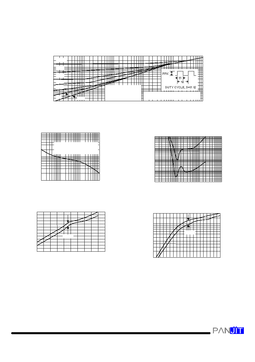
RATING AND CHARACTERISTICS CURVES
1SMB3EZ11 THRU 1SMB3EZ200
30
20
10
7
5
3
2
1
0.7
0.5
0.3
0.0001
0.0002
0.0005
0.001
0.002
0.005
0.01
0.02
0.05
0.1
0.2
0.5
1
2
5
10
D = 0.5
0.2
0.1
0.05
0.02
0.01
D = 0
NOTE BELOW 0.1 SECOND,
THERMAL RESPONSE
CURVE IS APPLICABLE TO
ANY LEAD LENGTH (L)
SINGLE PULSE
£G
TJL =
£K
JL(t)PPK
REPETITIVE PULSES
£G
TJL =
£K
JL(t,D)PPK
Fig. 2-TYPICAL THERMAL RESPONSE L,
1K
500
300
200
100
50
30
20
10
.1 .2 .3 5 1
2
3
5 10 20
50 100
RECTANGULAR NONREPETITIVE
WAVEFORM TJ = 25
¢J
PRIOR TO
INITIAL PULSE
P.W. PULSE WIDTH (ms)
0.1
0.05
0.03
0.02
0.01
0.005
0.003
0.002
0.001
0.0005
0.0003
0.0002
0.0001
1
2
5
10
20
50
100
200
500
1K
NOMINAL VZ (VOLTS)
Fig. 3-MAXIMUM SURGE POWER
Fig. 4-TYPICAL REVERSE LEAKAGE
8
6
4
2
0
-2
-4
3 4 6 8 10 12
RANGE
VZ, ZENER VOLTAGE @IZT (VOLTS)
200
100
50
40
30
20
10
0
20
40
60
80
100
120
140
160
180
200
RANGE
VZ, ZENER VOLTAGE @IZT (VOLTS)
Fig. 5-UNITS TO 12 VOLTS
Fig. 6-UNITS 10 TO 200 VOLTS
£c
J
L
(
t
,
D
)
T
R
A
N
S
I
E
N
T
T
H
E
R
M
A
L
R
E
S
I
S
T
A
N
C
E
J
U
N
C
T
I
O
N
-
T
O
-
L
E
A
D
(
¢J
/
W
)
P
P
K
,
P
E
A
K
S
U
R
G
E
P
O
W
E
R
(
W
A
T
T
S
)
I
R
,
R
E
V
E
R
S
E
L
E
A
D
A
G
E
(
u
A
d
c
)
@
V
R
A
S
S
P
E
C
I
F
I
E
D
I
N
E
L
E
C
.
C
H
A
R
.
T
A
B
L
E
£c
V
Z
,
T
E
M
P
E
R
A
T
U
R
E
C
O
E
F
F
I
C
I
E
N
T
(
m
V
/
¢J
)
@
I
Z
T
£c
V
Z
,
T
E
M
P
E
R
A
T
U
R
E
C
O
E
F
F
I
C
I
E
N
T
(
m
V
/
¢J
)
@
I
Z
T
RATING AND CHARACTERISTICS CURVES
1SMB3EZ11 THRU 1SMB3EZ200
100
50
30
20
10
5
3
2
1
0.5
0.3
0.2
0.1
0 1 2 3 4 5 6 7 8 9 10
VZ, ZENER VOLTAGE (VOLTS)
100
50
30
20
10
5
3
2
1
0.5
0.3
0.2
0.1
0
10
20
30
40
50
60 70
80
90 100
VZ, ZENER VOLTAGE (VOLTS)
Fig. 7-VZ = 3.9 THRU 10 VOLTS
Fig. 8-VZ = 12 THRU 82 VOLTS
100
50
30
20
10
5
3
2
1
0.5
0.3
0.2
0.1
100 120 140 160 180 200
VZ, ZENER VOLTAGE (VOLTS)
80
70
60
50
40
30
20
10
0
0 1/8 1/4 3/8 1/2 5/8 3/4 7/8 1
PRIMARY PATH OF
CONDUCTION IS THROUGH
THE CATHODE LEAD
L, LEAD LENGTH TO HEAT SINK (INCH)
Fig. 9-VZ = 100 THRU 200 VOLTS
Fig. 10-TYPICAL THERMAL RESISTANCE
I
Z
,
Z
E
N
E
R
C
U
R
R
E
N
T
(
m
A
)
I
Z
,
Z
E
N
E
R
C
U
R
R
E
N
T
(
m
A
)
I
Z
,
Z
E
N
E
R
C
U
R
R
E
N
T
(
m
A
)
£c
J
L
,
J
U
N
C
T
I
O
N
-
L
E
A
D
T
H
E
R
M
A
L
R
E
S
I
S
T
A
N
C
E
(
¢J
/
W
)

APPLICATION NOTE:
Since the actual voltage available from a given zener
diode is temperature dependent, it is necessary to
determine junction temperature under any set of
operating conditions in order to calculate its value. The
following procedure is recommended:
Lead Temperature, T
L
, should be determined from:
TL =
£c
LA
P
D
+ T
A
£c
LA
is the lead-to-ambient thermal resistance (
¢J
/W)
and P
D
is the power dissipation. The value for
£c
LA
will
vary and depends on the device mounting method.
£c
LA
is generally 30-40
¢J
/W for the various chips and
tie points in common use and for printed circuit board
wiring.
The temperature of the lead can also be measured using
a thermocouple placed on the lead as close as possible to
the tie point. The thermal mass connected to the tie point
is normally large enough so that it will not significantly
respond to heat surges generated in the diode as a result
of pulsed operation once steady-state conditions are
achieved. Using the measured value of T
L
, the junction
temperature may be determined by:
T
J
= T
L
+
£G
T
JL
£G
T
JL
is the increase in junction temperature above the
lead temperature and may be found from Figure 2 for a
train of power pulses or from Figure 10 for dc power.
£G
T
JL
=
£c
LA
P
D
For worst-case design, using expected limits of Iz, limits
of P
D
and the extremes of T
J
(
£G
T
JL
) may be estimated.
Changes in voltage, Vz, can then be found from:
£G
V =
£c
VZ
£G
T
J
£c
VZ
, the zener voltage temperature coefficient, is
found from Figures 5 and 6.
Under high power-pulse operation, the zener voltage
will vary with time and may also be affected significantly
be the zener resistance. For best regulation, keep current
excursions as low as possible.
Data of Figure 2 should not be used to compute surge
capability. Surge limitations are given in Figure 3. They
are lower than would be expected by considering only
junction temperature, as current crowding effects cause
temperatures to be extremely high in small spots resulting
in device degradation should the limits of Figure 3 be
exceeded.