 | –≠–ª–µ–∫—Ç—Ä–æ–Ω–Ω—ã–π –∫–æ–º–ø–æ–Ω–µ–Ω—Ç: TSP075A | –°–∫–∞—á–∞—Ç—å:  PDF PDF  ZIP ZIP |
PAGE . 1
DATE : SEP.02.2002
DATA SHEET
TSP058A~TSP320A
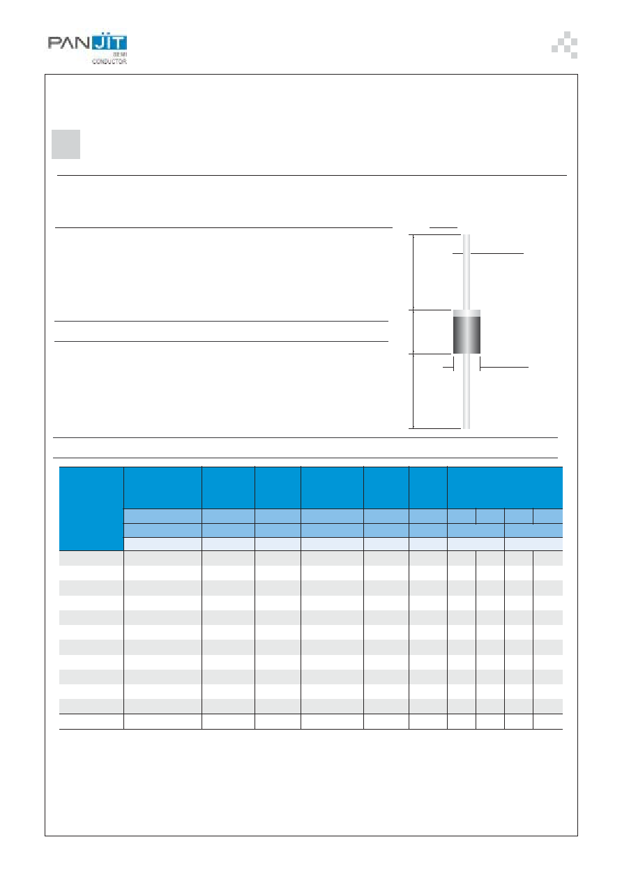
DO-15
Unit: inch ( mm )
.140(3.6)
.104(2.6)
.034(.86)
.028(.71)
1.0(25.4)
MIN.
.300(7.6)
.230(5.8)
1.0(25.4)
MIN.
SUMMARY ELECTRICAL CHARACTERISTICS
MECHANICAL DATA
∑ Case: JEDEC DO-15 molded plastic
∑ Te r m i n a l s : P l a t e d A x i a l l e a d s , s o l d e r a b l e p e r
MIL-STD-750, Method 2026
∑ Polarity: Bi-directional
∑ Weight: 0.015 ounce, 0.4 gram
FEATURES
∑ Protects by limiting voltages and shunting surge currents away from sensitive circuits
∑ Designed for telecommunications applications such as line cards, modems, PBX, FAX,
LAN,VHDSL
∑ Helps meet standards such as GR1089, ITU K.20, IEC950, UL1459&50, FCC part 68
∑ Low capacitance, High surge (A, B, C rating available), precise voltage limiting, Long life
AXIAL LEAD BI-DIRECTIONAL THYRISTOR SURGE PROTECTOR DEVICE
NOTES:
1. Specific V
DRM
values are available by request.
2. Specific I
H
values are available by request.
3. All ratings and characteristics are at 25 ∞C unless otherwise specified.
4. V
DRM
applies for the life of the device. I
DRM
will be in spec during and following operation of the device.
5. V
BO1
is at 100V/msec, I
SC
=10A
pk
, V
OC
=1KV
pk
, 10/1000 Waveform
6. V
BO2
is at f = 60 Hz, I
SC
= 1 A
(RMS)
, Vac = 1KV
(RMS)
, R
L
= 1 KW, 1/2 AC cycle
r
e
b
m
u
N
t
r
a
P
e
v
i
t
i
t
e
p
e
R
d
e
t
a
R
e
t
a
t
S
-
f
f
O
k
a
e
P
e
g
a
t
l
o
V
r
e
v
o
k
a
e
r
B
e
g
a
t
l
o
V
e
t
a
t
S
-
n
O
e
g
a
t
l
o
V
e
v
i
t
i
t
e
p
e
R
e
t
a
t
S
-
f
f
O
k
a
e
P
t
n
e
r
r
u
C
r
e
v
o
k
a
e
r
B
t
n
e
r
r
u
C
g
n
i
d
l
o
H
t
e
n
r
r
u
C
e
c
n
a
t
i
c
a
p
a
C
e
t
a
t
S
-
f
f
O
V
m
5
1
=
c
a
V
,
z
H
M
1
=
f
(
RMS
)
.
x
a
M
.
x
a
M
.
x
a
M
.
x
a
M
.
x
a
M
.
n
i
M
.
p
y
T
.
x
a
M
.
p
y
T
.
x
a
M
V
DRM
V
BO
I
@
BO
V
T
A
1
@
I
DRM
I
BO
I
H
C
O
V
0
@
c
d
C
O
V
0
5
@
c
d
V
V
V
µA
A
m
A
m
F
p
F
p
A
8
5
0
P
S
T
8
5
7
7
5
5
0
0
8
0
5
1
4
4
6
6
6
1
4
2
A
5
6
0
P
S
T
5
6
8
8
5
5
0
0
8
0
5
1
9
3
4
6
5
1
3
2
A
5
7
0
P
S
T
5
7
8
9
5
5
0
0
8
0
5
1
7
3
7
5
3
1
0
2
A
0
9
0
P
S
T
0
9
0
3
1
5
5
0
0
8
0
5
1
4
3
4
5
2
1
8
1
A
0
2
1
P
S
T
0
2
1
0
6
1
5
5
0
0
8
0
5
1
2
3
8
4
2
1
7
1
A
0
4
1
P
S
T
0
4
1
0
8
1
5
5
0
0
8
0
5
1
9
2
7
4
9
6
1
A
0
6
1
P
S
T
0
6
1
0
2
2
5
5
0
0
8
0
5
1
8
2
3
4
9
5
1
A
0
9
1
P
S
T
0
9
1
0
6
2
5
5
0
0
8
0
5
1
8
2
0
4
8
4
1
A
0
2
2
P
S
T
0
2
2
0
0
3
5
5
0
0
8
0
5
1
7
2
0
4
8
4
1
A
5
7
2
P
S
T
5
7
2
0
5
3
5
5
0
0
8
0
5
1
7
2
8
3
8
3
1
A
0
2
3
P
S
T
0
2
3
0
0
4
5
5
0
0
8
0
5
1
7
2
8
3
8
3
1
s
e
t
o
n
)
3
,
1
(
)
6
,
5
,
3
(
)
3
(
)
3
(
)
3
(
)
3
,
2
(
)
3
(
)
3
(
)
3
(
)
3
(

PAGE . 2
DATE : SEP.02.2002
Typical Capacitance v.s. Off-state Voltage
f=1 M
HZ
v =15mV
AC
d
RMS
T = 25 C
J
O
Capacitance
(pF)
V
Off-state Voltage (V)
D
Typical Capacitance v.s. Rated Repetitive Off-state Voltage
f=1 M
HZ
T = 25 C
J
O
v =15mV
AC
d
RMS
0
20
40
60
80
100
120
140
0.01
0.1
1
10
100
150
0.001
0.0001
I
O
f
f-State
Current
(
A)
D,
m
T ( C )
J
O
Typical Off-state Current v.s Junction Temperature
TSP220SB
TSP220SA
TSP220SC
25
0
25
50
75
100
125
100
150
200
250
300
T , Junction Temperature ( C)
J
O
Typical Holding Current
I
,
Holding
Current
(mA)
H
10A, 10/1000 microseconds
Capacitance
(pF)
V
DRM
20
30
40
50
60
50
100
150
200
250
300
350
0
10
V =0 Volts DC
D
V =50 Volts DC
D
0.1
1
10
100
5
10
15
20
25
30
TSP220SA
RATING AND CHARACTERISTIC CURVES
CAPACITANCE CHARACTERISTICS
F = 1 MHz, V
ac
= 15 mV
rms
r
e
b
m
u
N
t
r
a
P
e
c
n
a
t
i
c
a
p
a
C
e
t
a
t
S
-
f
f
O
C
O
F
p
c
d
V
0
c
d
V
1
c
d
V
2
c
d
V
5
c
d
V
0
5
.
p
y
T
.
x
a
M
.
p
y
T
.
x
a
M
.
p
y
T
.
x
a
M
.
p
y
T
.
x
a
M
.
p
y
T
.
x
a
M
A
8
5
0
P
S
T
4
4
6
6
0
4
1
5
6
3
9
4
3
3
4
4
6
1
4
2
A
5
6
0
P
S
T
9
3
4
6
5
3
9
4
1
3
7
4
8
2
2
4
5
1
3
2
A
5
7
0
P
S
T
7
3
7
5
3
3
2
4
9
2
0
4
6
2
5
3
3
1
0
2
A
0
9
0
P
S
T
4
3
4
5
0
3
9
3
6
2
7
3
3
2
2
3
2
1
8
1
A
0
2
1
P
S
T
2
3
8
4
8
2
3
3
4
2
1
3
1
2
6
2
2
1
7
1
A
0
4
1
P
S
T
9
2
7
4
5
2
2
3
1
2
0
3
8
1
5
2
9
6
1
A
0
6
1
P
S
T
8
2
3
4
5
2
7
2
1
2
4
2
8
1
0
2
9
5
1
A
0
9
1
P
S
T
8
2
0
4
4
2
5
2
0
2
3
2
7
1
8
1
8
4
1
A
0
2
2
P
S
T
7
2
0
4
3
2
5
2
9
1
3
2
6
1
8
1
8
4
1
A
5
7
2
P
S
T
7
2
8
3
3
2
4
2
9
1
2
2
6
1
7
1
8
3
1
A
0
2
3
P
S
T
7
2
8
3
3
2
4
2
9
1
2
2
6
1
7
1
8
3
1

PAGE . 3
DATE : SEP.02.2002
© Copyright PanjIt International Inc. 2001
All rights are reserved. Reproduction in whole or in part is prohibited without the prior written consent of the copyright owner.
The information presented in this document does not form part of any quotation or contract, is believed to be accurate and reliable and
may changed without notice. No liability will be accepted by the publisher for any consequence of its use.
Publication thereof does not convey nor imply any license under patent- or other industrial or intellectual property rights.
PanJit Internatioal Inc.
http://www.panjit.com.tw email: sales@panjit.com.tw
RATING AND CHARACTERISTIC CURVES
IMPORTANT NOTICE
This information is intended to unambiguously characterize the product in order to facilitate the customer's evaluation of the device in
the application. It will help the customer's technical experts determine that the device is compatible and interchangeable with similar
devices made by other vendors. The information in this data sheet is believed to be reliable and accurate. The specifications and
information herein are subject to change without notice. New products and improvements in products and their characterization are
constantly in process. This provides a superior performing and the highest value product. The factory should be consulted for the
most recent information and for any special characteristics not described or specified.
50
100
150
200
250
300
350
0.08
0.1
0.12
0.14
.16
T
emperature
Coef
ficient
of
V
,%/
C
DRM
o
Rated V
at T =25 C (V)
DRM
J
o
Temperature Coefficient of V
DRM
150
200
250
300
350
T , Junction Temperature ( C)
J
O
T
e
mperature
Coef
ficient
(mA/
C)
o
Typical Holding Current Temperature Coefficient
-1.0
-1.5
-2.0
-2.5
-3.0
-3.5
10A, 10/1000 microseconds
-0.1
-1.0
-1.5
-2.0
-2.5
-3.0
-25
T , Junction Temperature ( C)
J
O
0
25
50
75
100
125
T
e
mperature
Coef
ficient
(mA/
C)
o
Typical Holding Current Temperature Coefficient
10A, 10/1000 microseconds

PAGE . 4
DATE : SEP.02.2002
SELECTION GUIDE
Follow these steps to select the proper Thyristor surge protector for your application:
1. Define the operating parameters for the circuit:
∑ Ambient operating temperature range
∑ Maximum telephone line operating current (highest battery and shortest copper loop)
∑ Maximum operating voltage: (Maximum DC bias + peak ringing voltage)
∑ Maximum surge current
∑ System voltage damage threshold
∑ Select device with an off-state voltage rating (V
DRM
) above the maximum operating voltage at the minimum operating temperature.
3. Select surge current ratings (I
PPS
and I
TSM
) ≥ those which the application must withstand.
4. Verify that the minimum holding current of the device at the maximum ambient temperature is above the maximum dc current of the
system.
5. Verify that the maximum breakover voltage of the device is below the system damage threshold.
6. Verify that the circuit's ambient operating temperatures are within the device's operating temperature range.
7. Verify that the device's dimensions fit the application's space considerations.
8. Independently evaluate and test the suitability and performance of the device in the application
g
n
i
t
a
R
t
n
e
r
r
u
C
e
s
l
u
P
k
a
e
P
e
v
i
t
i
t
e
p
e
R
-
n
o
N
k
a
e
P
e
v
i
t
i
t
e
p
e
R
-
n
o
N
t
n
e
r
r
u
C
e
g
r
u
S
e
t
a
t
S
-
n
O
l
o
b
m
y
S
I
PPS
I
TSM
e
v
a
W
t
n
e
r
r
u
C
t
i
u
c
r
i
C
-
t
r
o
h
S
0
1
/
2
µs
0
2
/
8
µs
0
6
1
/
0
1
µs
0
1
3
/
5
µs
0
6
5
/
0
1
µs
0
0
0
1
/
0
1
µs
A
0
2
e
v
a
W
e
g
a
t
l
o
V
t
i
u
c
r
i
C
-
n
e
p
O
0
1
/
2
µs
0
5
/
2
.
1
µs
0
6
1
/
0
1
µs
0
0
7
/
0
1
µs
0
6
5
/
0
1
µs
0
0
0
1
/
0
1
µs
e
u
l
a
V
A
5
7
1
A
0
5
1
A
0
0
1
A
5
8
A
0
7
A
0
5
s
e
t
o
N
)
6
,
5
,
4
,
2
,
1
(
)
4
,
3
,
2
,
1
(
MAXIMUM SURGE RATINGS (T
J
= 25 ∞C UNLESS OTHERWISE NOTED)
Notes:
1. Thermal accumulation between successive surge tests is
not allowed.
2 . T h e d e v i c e u n d e r t e s t i n i t i a l l y m u s t b e i n t h e r m a l
equilibrium with T
J
= 25 ∞C.
3. Test at 1 cycle, 60 Hz.
4. Surge ratings are non-repetitive because instantaneous
junction temperatures may exceed the maximum rated T
J
.
Nevertheless, devices will survive many surge applications
without degradation. Surge capability will not degrade over
a device's typical operating life.
5. Adjust the surge generator for optimum current-wave
a c c u r a c y w h e n b o t h v o l t a g e a n d c u r r e n t w a v e
specifications cannot be exactly met. The current wave is
more important than the voltage wave for accurate surge
evaluation.
6. The waveform is defined as A/B ms where:
A: (Virtual front time) = 1.25 X Rise time = 1.25 X (T
b
- T
a
)
B (Duration time to 50% level of Ipps) = T
1
- T
0
0%
20%
40%
60%
80%
100%
Time
% Ipps
Tb
Ta
T1
To

PAGE . 5
DATE : SEP.02.2002
g
n
i
t
a
R
l
o
b
m
y
S
e
u
l
a
V
t
i
n
U
e
g
n
a
R
e
r
u
t
a
r
e
p
m
e
T
n
o
i
t
c
n
u
J
e
g
a
r
o
t
S
T
STG
0
5
1
o
t
0
5
-
O
C
e
g
n
a
R
e
r
u
t
a
r
e
p
m
e
T
n
o
i
t
c
n
u
J
g
n
i
t
a
r
e
p
O
T
J
0
5
1
o
t
0
4
-
O
C
e
g
n
a
R
e
r
u
t
a
r
e
p
m
e
T
t
n
e
i
b
m
A
g
n
i
t
a
r
e
p
O
T
a
5
6
o
t
0
4
-
O
C
Notes:
PCB board mounted on minimum foot print.
MAXIMUM THERMAL RATINGS
c
i
t
s
i
r
e
t
c
a
r
a
h
C
l
o
b
m
y
S
e
u
l
a
V
t
i
n
U
T
s
d
a
e
L
o
t
n
o
i
t
c
n
u
J
e
c
n
a
t
s
i
s
e
R
l
a
m
r
e
h
T
L
o
t
t
n
e
c
a
j
d
a
b
a
t
n
o
.
s
e
z
i
s
d
a
p
l
a
c
i
t
n
e
d
i
o
t
d
e
r
e
d
l
o
s
s
d
a
e
l
h
t
o
B
.
c
i
t
s
a
l
p
R
L
J
0
2
.
x
a
M
O
W
/
C
THERMAL CHARACTERISTICS
Notes:
The junction to lead thermal resistance represents a minimum limiting value with both leads soldered to a large near-infinite heatsink. The
junction to ambient thermal resistance depends strongly on board mounting conditions and typically is 3 to 6 times higher than the junction
to lead resistance. The data shown is to be used as guideline values for preliminary engineering.
ELECTRICAL CHARACTERISTICS (T
C
= 25∞C UNLESS OTHERWISE NOTED)
s
r
e
t
e
m
a
r
a
P
s
n
o
i
t
i
d
n
o
C
t
s
e
T
l
o
b
m
y
S
.
n
i
M
.
x
a
M
t
i
n
U
k
a
e
P
e
v
it
it
e
p
e
R
t
n
e
r
r
u
C
e
t
a
t
S
-
f
f
O
V
D
V
d
e
t
a
r
=
DRM
I
DRM
5
µA
t
n
e
r
r
u
C
r
e
v
o
k
a
e
r
B
I
,
z
H
0
6
=
f
SC
V
,
s
m
r
A
1
=
c
a
R
,
s
m
r
V
K
1
=
L
K
1
=
e
l
c
y
c
C
A
2
/
1
,
I
O
B
0
0
8
A
m
1
t
n
e
r
r
u
C
g
n
i
d
l
o
H
0
0
0
1
/
0
1
µ
I
,
m
r
o
f
e
v
a
w
s
C
S
V
,
A
0
1
=
C
O
R
,
V
2
6
=
L
0
0
4
=
I
H
0
5
1
A
m
e
g
a
tl
o
V
e
t
a
t
S
-
n
O
I
T
0
0
3
=
w
T
,
A
1
=
µ
e
s
l
u
p
1
,
s
V
T
5
V
Notes:
Specific I
H
values are available by request.

PAGE . 6
DATE : SEP.02.2002
c
i
t
s
i
r
e
t
c
a
r
a
h
C
l
o
b
m
y
S
e
u
l
a
V
V
BO
e
g
a
t
l
o
V
r
e
v
o
k
a
e
r
B
d
e
r
u
s
a
e
m
n
w
o
d
k
a
e
r
b
t
a
r
o
n
i
e
c
i
v
e
d
e
h
t
s
s
o
r
c
a
e
g
a
t
l
o
v
m
u
m
i
x
a
M
e
s
i
r
f
o
e
t
a
r
t
n
e
r
r
u
c
d
n
a
e
g
a
t
l
o
v
d
e
i
f
i
c
e
p
s
a
r
e
d
n
u
I
BO
t
n
e
r
r
u
C
r
e
v
o
k
a
e
r
B
V
(
e
g
a
t
l
o
v
r
e
v
o
k
a
e
r
b
e
h
t
t
a
g
n
i
w
o
l
f
t
n
e
r
r
u
c
s
u
o
e
n
a
t
n
a
t
s
n
I
BO
)
I
H
t
n
e
r
r
u
C
g
n
i
d
l
o
H
e
t
a
t
s
-
n
o
e
h
t
n
i
e
c
i
v
e
d
e
h
t
n
i
a
t
n
i
a
m
o
t
d
e
r
i
u
q
e
r
t
n
e
r
r
u
c
m
u
m
i
n
i
M
I
T
t
n
e
r
r
u
c
e
t
a
t
s
-
n
O
n
o
i
t
i
d
n
o
c
e
t
a
t
s
-
n
o
e
h
t
n
i
e
c
i
v
e
d
e
h
t
h
g
u
o
r
h
t
t
n
e
r
r
u
C
V
T
e
g
a
t
l
o
v
e
t
a
t
s
-
n
O
d
e
i
f
i
c
e
p
s
a
t
a
n
o
i
t
i
d
n
o
c
e
t
a
t
s
-
n
o
e
h
t
n
i
e
c
i
v
e
d
e
h
t
s
s
o
r
c
a
e
g
a
t
l
o
V
(
t
n
e
r
r
u
c
I
T
)
V
DRM
e
g
a
t
l
o
V
e
t
a
t
S
-
f
f
O
k
a
e
P
e
v
i
t
i
t
e
p
e
R
d
e
t
a
R
ll
a
g
n
i
d
u
l
c
n
i
,
e
g
a
t
l
o
v
e
t
a
t
s
-
f
f
o
e
h
t
f
o
e
u
l
a
v
s
u
o
e
n
a
t
n
a
t
s
n
i
t
s
e
h
g
i
h
e
h
T
t
n
e
i
s
n
a
r
t
e
v
i
t
i
t
e
p
e
r
n
o
n
ll
a
g
n
i
d
u
l
c
x
e
t
u
b
s
e
g
a
t
l
o
v
t
n
e
i
s
n
a
r
t
e
v
i
t
i
t
e
p
e
r
s
e
g
a
t
l
o
v
I
DRM
t
n
e
r
r
u
C
e
t
a
t
S
-
f
f
O
k
a
e
P
e
v
i
t
i
t
e
p
e
R
n
o
i
t
a
c
il
p
p
a
e
h
t
m
o
r
f
s
t
l
u
s
e
r
t
a
h
t
t
n
e
r
r
u
c
f
o
e
u
l
a
v
)
k
a
e
p
(
m
u
m
i
x
a
m
e
h
T
V
f
o
DRM
I
PPS
t
n
e
r
r
u
c
e
s
l
u
p
k
a
e
P
e
v
i
t
i
t
e
p
e
R
-
n
o
N
e
d
u
t
il
p
m
a
d
e
i
f
i
c
e
p
s
f
o
t
n
e
r
r
u
c
e
s
l
u
p
m
i
k
a
e
p
f
o
e
u
l
a
v
m
u
m
i
x
a
m
d
e
t
a
R
e
c
i
v
e
d
e
h
t
o
t
e
g
a
m
a
d
t
u
o
h
t
i
w
d
e
il
p
p
a
e
b
y
a
m
t
a
h
t
e
p
a
h
s
e
v
a
w
d
n
a
t
s
e
t
r
e
d
n
u
t
d
/
i
d
t
n
e
r
r
u
c
e
t
a
t
s
-
n
o
f
o
e
s
i
r
f
o
e
t
a
r
l
a
c
i
t
i
r
C
d
n
a
t
s
h
t
i
w
n
a
c
e
c
i
v
e
d
e
h
t
t
a
h
t
t
n
e
r
r
u
c
f
o
e
s
i
r
f
o
e
t
a
r
e
h
t
f
o
e
u
l
a
v
d
e
t
a
R
.
e
g
a
m
a
d
t
u
o
h
t
i
w
t
d
/
v
d
e
g
a
t
l
o
V
e
t
a
t
S
-
f
f
O
f
o
e
s
i
R
f
o
e
t
a
R
l
a
c
i
t
i
r
C
V
w
o
l
e
b
(
e
g
a
t
l
o
v
f
o
e
s
i
r
f
o
e
t
a
r
m
u
m
i
x
a
m
e
h
T
DRM
e
s
u
a
c
t
o
n
ll
i
w
t
a
h
t
)
.
e
t
a
t
s
-
n
o
e
h
t
o
t
e
t
a
t
s
-
f
f
o
e
h
t
m
o
r
f
g
n
i
h
c
t
i
w
s
V
BO
V
BR
V
DRM
V
T
I
PPS
I
TSM
I
T
I
BO
I
H
I
BR
I
DRM
_V
+V
_I
+I