 | –≠–ª–µ–∫—Ç—Ä–æ–Ω–Ω—ã–π –∫–æ–º–ø–æ–Ω–µ–Ω—Ç: 3291-11 | –°–∫–∞—á–∞—Ç—å:  PDF PDF  ZIP ZIP |
Page 1 of 15
Document No. 70-0009-04
www.psemi.com
©2005 Peregrine Semiconductor Corp. All rights reserved.
The PE3291 is a dual fractional-N FlexiPower
TM
phase-lock loop
(PLL) IC designed for frequency synthesis. Each PLL includes
a FlexiPower
TM
prescaler, phase detector, charge pump and on-
board fractional spur compensation.
The FlexiPower
prescalers are supplied power on dedicated
pins and can operate at a substantial power savings at
voltages as low as 0.8 volts, while allowing a 3 volt charge
pump supply. For 3 volt only systems, on-chip voltage
regulation may be used to generate the prescaler power
supplies.
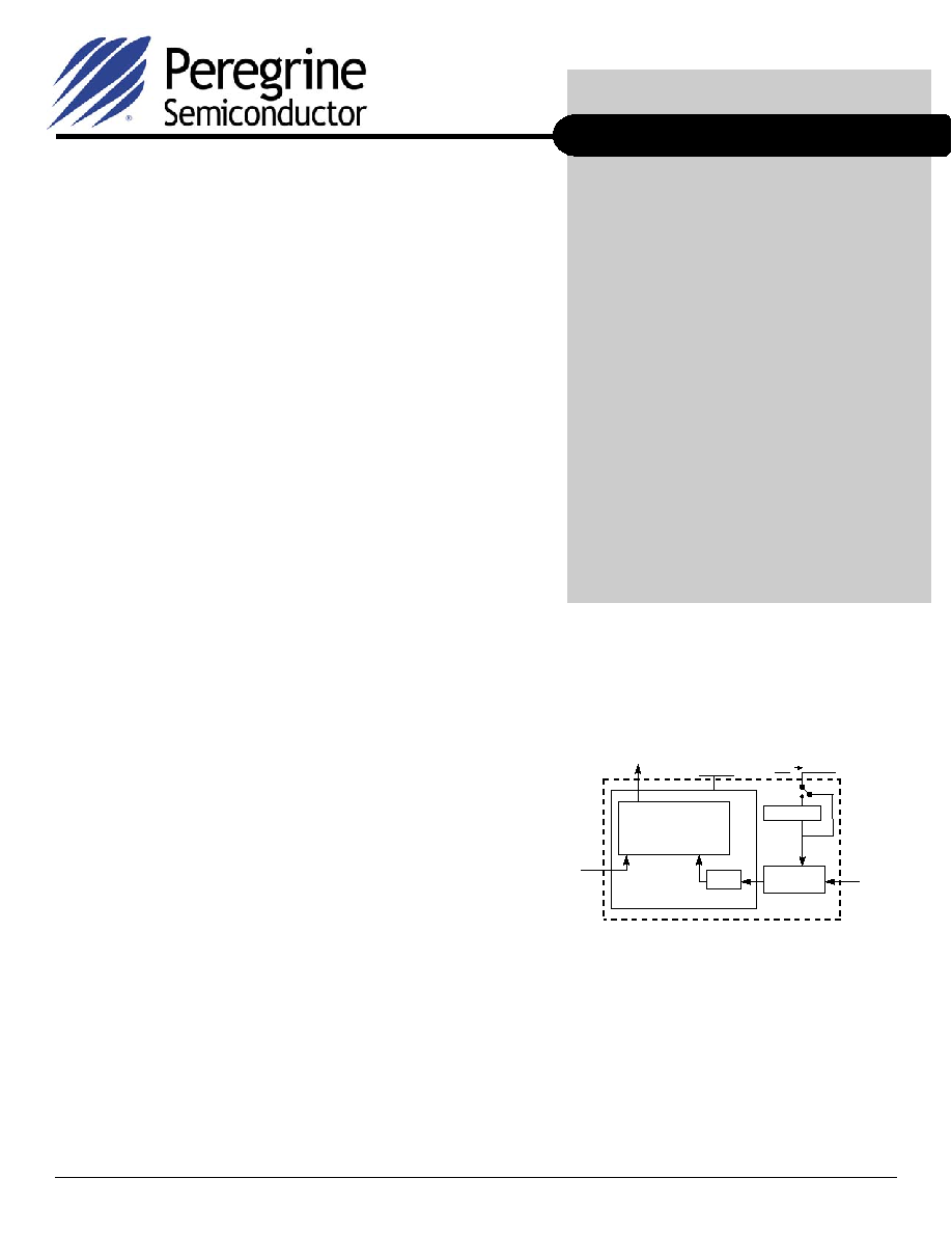
Figure 1 illustrates the implementation of the FlexiPower
technology. The prescaler power supply may be provided
externally or internally regulated down from V
DD
. In a typical
950 MHz application the total current consumed by the PLL is
2.1 mA. Operation at reduced current levels provides
significant battery life extension. The PE3291 allows the
system designer to minimize power consumption by controlling
the voltage on the prescaler. For additional operating speeds
and current consumptions refer to Figures 5 and 6.
PE3291 provides fractional-N division with power-of-two
denominator values up to 32. This allows comparison
frequencies up to 32 times the channel spacing, providing a
lower phase noise floor than integer PLLs. The 32/33 RF
prescaler (PLL1) operates up to 1200 MHz and the 16/17 IF
prescaler (PLL2) operates up to 550 MHz.
The PE3291 Phase Locked-Loop is manufactured on
Peregrine's UltraCMOSTM process, a patented variation of
silicon-on-insulator (SOI) technology on a sapphire substrate,
offering the performance of GaAs with the economy and
integration of conventional CMOS.
Product Specification
1200 MHz / 550 MHz Dual
Fractional-N FlexiPowerTM PLL
for Frequency Synthesis
Product Description
PE3291
Features
∑
Ultra-Low Power via FlexiPower
variable supply voltages
∑
Modulo-32 fractional-N main counters
∑
On-board fractional spur compensation:
No tuning required, stable over
temperature
∑
Improved phase noise compared to
integer-N architectures
Figure 1:
FlexiPower technology enables
the prescaler to operate at voltages down to
0.8 volts. This significantly reduces the total
power.
PE3291
Low
Speed Counters
Phase Comparator
and
Charge pump
Ref.
Input
To Loop Filter
3 Volts
Prescaler
0.8 3 Volts
Regulator
Applications
∑
CDMA handsets
∑
CDMA base stations
∑
Analog Cordless phones
∑
One and two way pagers
Product Specification
PE3291
Page 2 of 15
©2005 Peregrine Semiconductor Corp. All rights reserved.
Document No. 70-0009-04
UltraCMOSTM RFIC Solutions
Table 1. Pin Descriptions
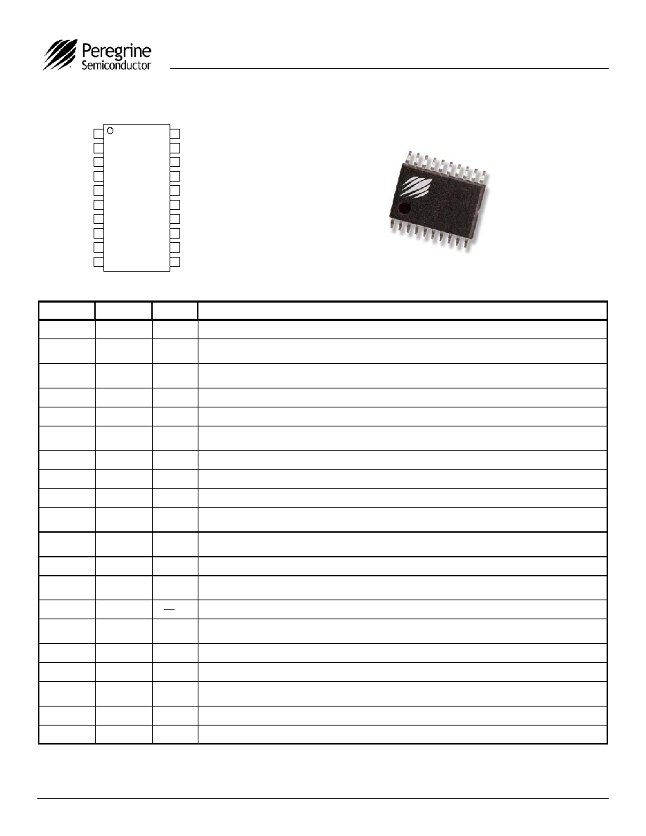
Figure 2. Pin Configurations (Top View)
Figure 3. Package Type
20-lead TSSOP
N/C
1
V
DD
2
CP1
3
GND
4
f
in
1
5
Dec1
6
V
DD
1
7
f
r
8
GND
9
f
o
LD 10
Clock
11
Data
12
LE
13
V
DD
2
14
Dec2
15
f
in
2
16
GND
17
CP2
18
V
DD
19
V
DD
20
Pin No.
Pin Name
Type
Description
1
N / C
No connect.
2
V
DD
(Note 1)
Power supply voltage input. Input may range from 2.7 V to 3.3 V. A bypass capacitor should be placed
as close as possible to this pin and be connected directly to the ground plane.
3
CP1
Output
Internal charge-pump output from PLL1 for connection to a loop filter for driving the input of an external
VCO.
4
GND
Ground.
5
f
in
1
Input
Prescaler input from the PLL1 (RF) VCO. Maximum frequency is 1.2 GHz.
6
Dec1
Power supply decoupling pin for PLL1. A capacitor should be placed as close as possible to this pin and
be connected directly to the ground plane.
7
V
DD1
PLL1 prescaler power supply (FlexiPower 1).
8
f
r
Input
Reference frequency input.
9
GND
Ground.
10
f
o
LD
Output
Multiplexed output of the PLL1 and PLL2 main counters or reference counters, Lock Detect signals, and
data out of the shift register. CMOS output (see Table 11, f
o
LD Programming Truth Table).
11
Clock
Input
CMOS clock input. Serial data for the various counters is clocked in on the rising edge into the 21-bit shift
register.
12
Data
Input
Binary serial data input. CMOS input data entered MSB first. The two LSBs are the control bits.
13
LE
Input
Load Enable CMOS input. When LE is high, data word stored in the 21-bit serial shift register is loaded
into one of the four appropriate latches (as assigned by the control bits).
14
V
DD2
Output
PLL2 prescaler power supply (FlexiPower 2).
15
Dec2
Output
Power supply decoupling pin for PLL2. A capacitor should be placed as close as possible to this pin and
be connected directly to the ground plane.
16
F
in
2
Input
Prescaler input from the PLL2 (IF) VCO. Maximum frequency is 550 MHz.
17
GND
Ground.
18
CP2
Output
Internal charge-pump output for PLL2. For connection to a loop filter for driving the input of an external
VCO.
19
V
DD
(Note 1)
Same as pin 2.
20
V
DD
(Note 1)
Same as pin 2.
Note 1: V
DD
pins 2, 19, and 20 are connected by diodes and must be supplied with the same voltage level.
Product Specification
PE3291
Page 3 of 15
Document No. 70-0009-04
www.psemi.com
©2005 Peregrine Semiconductor Corp. All rights reserved.
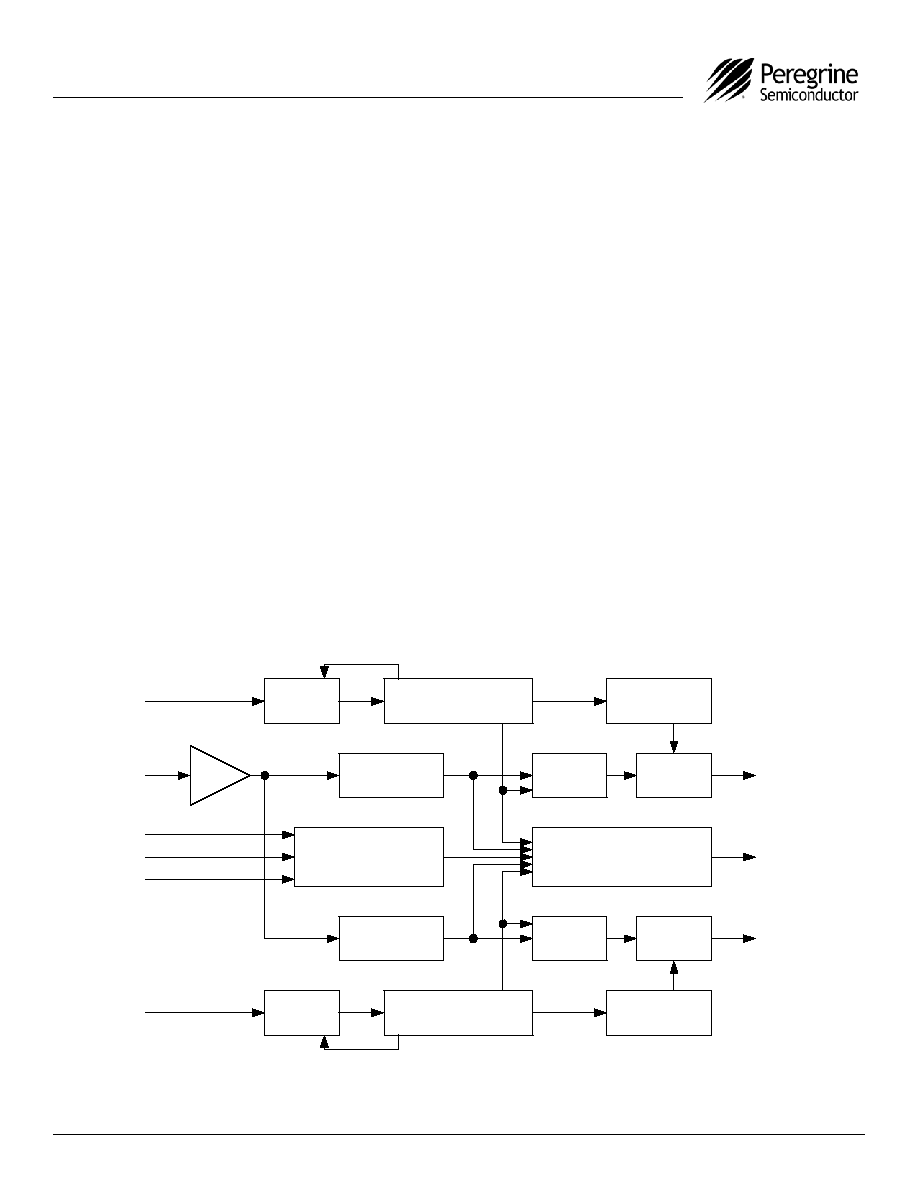
PE3291 Description
The PE3291 is intended for such applications as
the local oscillator for the RF and first IF of dual-
conversion transceivers. The RF PLL (PLL1)
includes a 32/33 prescaler with a 1200 MHz
maximum frequency of operation, where the IF
PLL (PLL2) incorporates a 16/17 prescaler with a
550 MHz maximum frequency of operation. Using
an advanced fractional-N phase-locked loop
technique, the PE3291 can generate a stable,
very low phase-noise signal. The dual fractional
architecture allows fine resolution in both PLLs,
with no degradation in phase noise performance.
Data is transferred into the PE3291 via a three-
wire interface (Data, Clock, LE). Supply voltage
can range from 2.7 to 3.3 volts for V
DD
and from
0.8 to 3.3 volts for the FlexiPower supply. PE3291
features very low power consumption and is
available in a 20-lead TSSOP (JEDEC MO-153-
AC) package.
FlexiPower Operation
Each FlexiPower PLL prescaler can be supplied
its own dedicated supply voltage as low as 0.8
volts for substantial power savings. The maximum
frequency of operation scales with the FlexiPower
supply voltage. If voltages less than V
DD
are not
available, the FlexiPower supplies can be
internally generated, but the power savings will
not be as great as when using external
FlexiPower supplies.
Spurious Response
A critical parameter for synthesizer designs is
spurious output. Spurs occur at the integer
multiples of the step size away from center tone.
An important feature of fractional synthesizers is
their ability to reduce these spurious sidebands.
The PE3291 has a built-in method for reducing
these spurs, with no external components or
tuning required. In addition, this circuitry works
over the full commercial temperature range.
Figure 4. PE3291 Block Diagram
32/33
Prescaler
f
in
1
19-bit Fractional-N
Main Divider
Fractional Spur
Compensation
Fractional Spur
Compensation
18-bit Fractional-N
Main Divider
9-bit Reference
Divider
9-bit Reference
Divider
21-bit Serial Control
Interface
Ref.
Amp.
f
r
Clock
Data
LE
f
in
2
16/17
Prescaler
f
o
LD
CP1
CP2
Phase
Detector
Phase
Detector
Charge
Pump
Charge
Pump
Multiplexer

Product Specification
PE3291
Page 4 of 15
©2005 Peregrine Semiconductor Corp. All rights reserved.
Document No. 70-0009-04
UltraCMOSTM RFIC Solutions
Table 5. DC Characteristics:
V
DD
= 3.0 V, -40∞ C < T
A
< 85∞ C, unless otherwise specified
Table 2. Absolute Maximum Ratings
Note 1: Periodically sampled, not 100% tested. Tested per MIL-
STD-883,
M3015
C2
Table 4. ESD Ratings
Electrostatic Discharge (ESD) Precautions
When handling this UltraCMOSTM device, observe the
same precautions that you would use with other ESD-
sensitive devices. Although this device contains
circuitry to protect it from damage due to ESD,
precautions should be taken to avoid exceeding the
specified rating in Table 4.
Latch-Up Avoidance
Unlike conventional CMOS devices, UltraCMOSTM
devices are immune to latch-up.
Symbol Parameter/Conditions
Min
Max
Units
V
DD
Supply
voltage
-0.3
4.0 V
V
I
Voltage on any input
-0.3
V
DD
+ 0.3
V
I
I
DC into any input
-10
+10
mA
I
O
DC into any output
-10
+10
mA
T
stg
Storage
temperature
range
-65 150 ∞C
Symbol Parameter/Conditions Min Max Units
V
DD
Supply
voltage
2.7
3.3 V
T
A
Operating
ambient
-40
85 ∞C
Table 3. Operating Ratings
Symbol Parameter/Conditions Level
Units
V
ESD
ESD voltage human body model
1000
V
Symbol Parameter
Conditions
Min
Typ
Max
Units
I
DD
3 V supply current when V
DD1
and V
DD2
are internally
regulated down from V
DD
(note 1)
(10 MHz Ref. Freq.)
P
2
, P
1
= 01 RF
RF PLL1 low speed
1.4
mA
P
2
, P
1
= 1X
RF PLL1 high speed
C
10
, C
20
= 01
IF PLL2 off
2.0
mA
P
2
, P
1
= 01
RF PLL1 low speed
C
10
, C
20
= 00
IF PLL2 low speed
2.1
mA
P
2
, P
1
= 10
RF PLL1 high speed
C
10
, C
20
= 00
IF PLL2 low speed
2.7
mA
P
2
, P
1
= 11
RF PLL1 high speed
C
10
, C
20
= 00
IF PLL2 high speed
3.1
mA
I
DD
3 V supply current when V
DD1
and V
DD2
are externally
supplied (note 1)
P
2
, P
1
= 00
2 PLL's enabled
1
PLL
enabled
1.0
0.7
mA
mA
I
DD1
PLL1 FlexiPower Prescaler
supply current (see fig. 5)
P
2
, P
1
= 00
PLL1 enabled
V
DD1
= 1/0 volt
V
DD1
= 1.8 volts
V
DD1
= 2.7 volts
0.5
1.5
4.0
mA
mA
mA
I
DD2
PLL2 FlexiPower Prescaler
supply current (see fig. 5)
P2, P1 = 00
PLL2 enabled
V
DD2
= 1.0 volt
V
DD2
= 1.8 volts
V
DD2
= 2.7 volts
0.4
1.2
2.0
mA
mA
mA
I
stby
Total standby current
5
50
mA
Digital inputs: Clock, Data, LE
V
IH
High level input voltage
V
DD
= 2.7 to 3.3 volts
0.7 x V
DD
V
V
IL
Low level input voltage
V
DD
= 2.7 to 3.3 volts
0.3 x V
DD
V
I
IH
High level input current
V
IH
= V
DD
= 3.3 volts
-1
+1
mA
I
IL
Low level input current
V
IL
= 0, V
DD
= 3.3 volts
-1
+1
mA
Absolute Maximum Ratings are those values listed in
the above table. Exceeding these values may cause
permanent device damage. Functional operation
should be restricted to the limits in the DC and AC
Characteristics table. Exposure to absolute maximum
ratings for extended periods may affect device
reliability.
Note 1: The total current consumed by the device is I
DD
when internal regulation is employed and I
DD
+ I
DD1
+ I
DD2
when V
DD1
and V
DD2
are
externally supplied. When V
DD1
and V
DD2
are internally generated, pins 7 and 14 should be left floating.

Product Specification
PE3291
Page 5 of 15
Document No. 70-0009-04
www.psemi.com
©2005 Peregrine Semiconductor Corp. All rights reserved.
Table 5. DC Characteristics (continued):
V
DD
= 3.0 V, -40∞ C < T
A
< 85∞ C, unless otherwise specified
Symbol Parameter
Conditions
Min
Typ
Max
Units
Reference Divider input: f
r
I
IHR
Input
current
V
IH
= V
DD
= 3.6 volts
+25
mA
I
ILR
Input
current
V
IL
= 0, V
DD
= 3.6 volts
-25
mA
Digital output: f
o
LD
V
OLD
Output
voltage
LOW
I
out
= 1 mA
V
V
OHD
Output voltage HIGH
I
out
= -1 mA
V
DD
-0.4
V
Charge Pump outputs: CP1, CP2
I
CP - Source
Drive current
VC
P
= V
DD
/ 2
-70
mA
I
CP - Sink
70
mA
I
CPL
Leakage current
0.5 V < V
CP
< V
DD
-0.5 volt
-5
5
nA
I
CP ≠ Source
vs.
Sink vs. Source mismatch
V
CP
= V
DD
/ 2, T
A
= 25∞ C
10 %
I
CP
vs. T
A
Output current vs. temperature
V
CP
= V
DD
/ 2
10
%
I
CP
vs. V
CP
Output current magnitude variation vs.
voltage
0.5 V < V
CP
< V
DD
≠ 0.5
volt, T
A
= 25∞ C
10
%
Figure 5. Prescaler Current vs. FlexiPower Voltage (V
DD1
and V
DD2
externally supplied)
0.8
1.2
1.6
2
2.4
2.8
3.2
FlexiPower voltage (V
DD1
, V
DD2
)
3.00
2.00
1.00
0.00
4.00
Ty
p
i
c
a
l
C
u
r
r
e
n
t
(m
A
)
PLL1
PLL2
Symbol Parameter
Conditions
Min
Max
Units
Control Interface and Latches (see figure 8)
f
Clk
Serial data clock frequency
10
MHz
t
ClockH
Serial clock HIGH time
50
ns
t
ClockL
Serial clock LOW time
50
ns
t
DSU
Data set-up time to Clock rising edge
50
ns
t
DHLD
Data hold time after Clock rising edge
10
ns
t
LEW
LE pulse width
50
ns
t
CLE
Clock falling edge to LE rising edge
50
ns
t
LEC
LE falling edge to Clock rising edge
50
ns
t
Data Out
Data Out delay after Clock falling edge (f
o
LD pin)
C
L
= 50 pf
90
ns
Table 6. AC Characteristics:
V
DD
= 3.0 V, -40∞ C < T
A
< 85∞ C, unless otherwise specified