 | –≠–ª–µ–∫—Ç—Ä–æ–Ω–Ω—ã–π –∫–æ–º–ø–æ–Ω–µ–Ω—Ç: 4263-10 | –°–∫–∞—á–∞—Ç—å:  PDF PDF  ZIP ZIP |
Page 1 of 4
Document No. 70-0175-02
www.psemi.com
©2005 Peregrine Semiconductor Corp. All rights reserved.
NDA required for full version: Contact sales@psemi.com
The PE4263 SP6T RF UltraCMOSTM Switch
addresses the specific design needs of the
Quad-Band GSM Handset Antenna Switch
Module Market. On-chip CMOS decode logic
facilitates three-pin low voltage CMOS control.
High ESD tolerance of 1500 V at all ports, no
blocking capacitor requirements and on-chip
SAW filter over-voltage protection devices
make this the ultimate in integration and
ruggedness.
The PE4263 UltraCMOSTM RF Switch is
manufactured in Peregrine's patented Ultra
Thin Silicon (UTSi
Æ
) CMOS process, offering
the performance of GaAs with the economy
and integration of conventional CMOS.
Product Specification
SP6T UltraCMOSTM 2.6 V Switch
100 ≠ 3000 MHz
Product Description
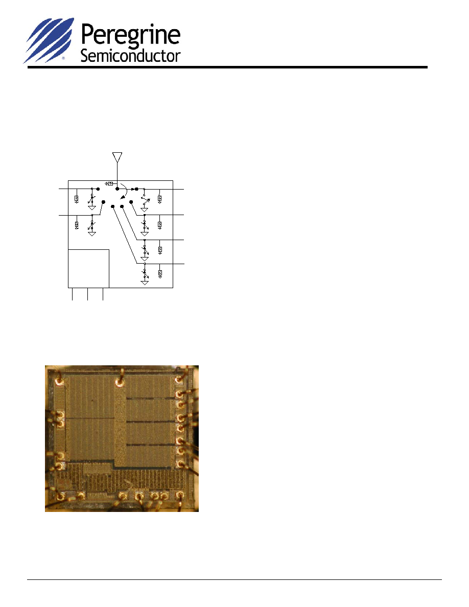
Figure 1. Functional Diagram
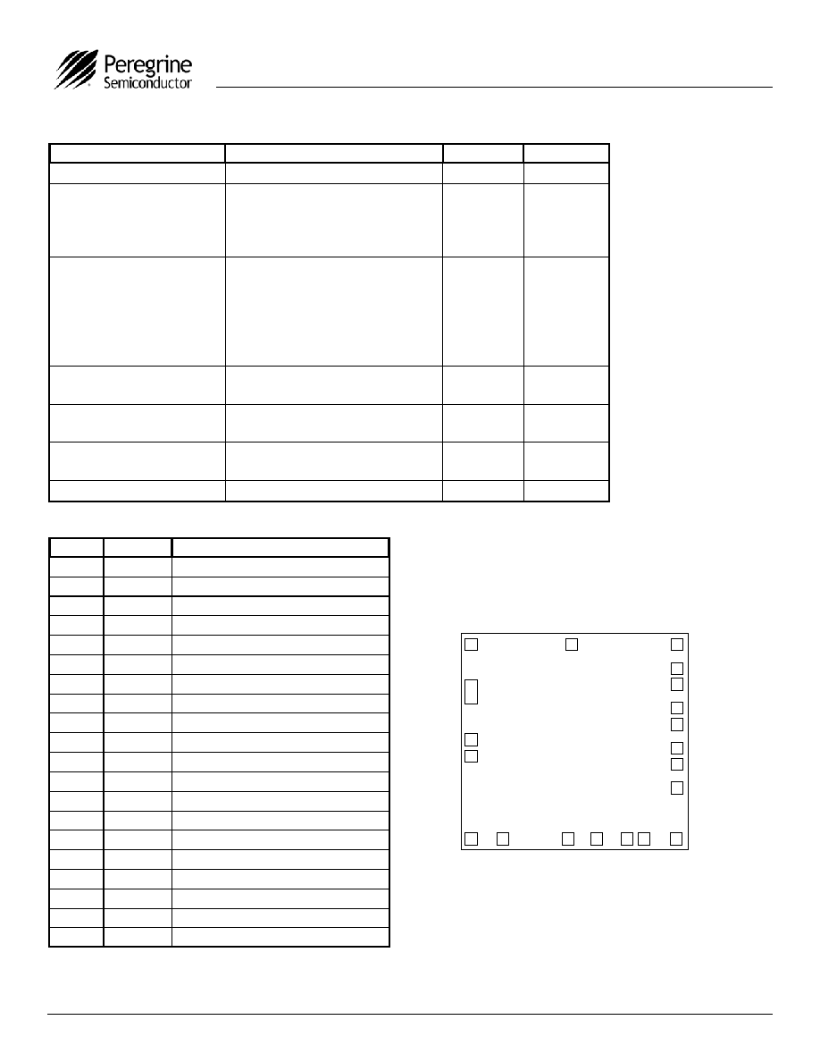
Figure 2. Die Top View
PE4263 DIE
Features
ANT
TX1
TX2
GND
GND
RX1
GND
RX2
GND
RX3
GND
RX4
GND
GND
VDD
V3
GND
V2
V1
GND
GND
RX1
RX2
RX3
RX4
TX1
TX2
CMOS
Control/Driver
and ESD
V1
V2
V3
∑
Three pin CMOS logic control with
integral decoder/driver
∑
Low TX insertion loss: 0.55 dB at 900
MHz, 0.65 dB at 1900 MHz
∑
TX ≠ RX Isolation of 48 dB at 900 MHz,
40 dB at 1900 MHz
∑
Low harmonics: 2f
o
= -85 dBc and
3f
o
= -72 dBc
∑
1500 V HBM ESD tolerance all ports
∑
41 dBm P1dB
∑
No blocking capacitors required
Product Specification
PE4263
Page 2 of 4
©2005 Peregrine Semiconductor Corp. All rights reserved.
Document No. 70-0175-02
UltraCMOSTM RFIC Solutions
NDA required for full version: contact sales@psemi.com
Table 1. Electrical Specifications @ +25 ∞C, V
DD
= 2.6 V (Z
S
= Z
L
= 50
)
Parameter
Conditions
Typical
Units
Operational Frequency
MHz
Insertion Loss
ANT - TX - 850 / 900 MHz
ANT - TX - 1800 / 1900 MHz
ANT - RX - 850 / 900 MHz
ANT - RX - 1800 / 1900 MHz
0.55
0.65
0.90
1.00
dB
dB
dB
dB
Isolation
TX - RX - 850 / 900 MHz
TX - RX - 1800 / 1900 MHz
TX - TX - 850 / 900 MHz
TX - TX - 1800 / 1900 MHz
ANT - TX - 850 / 900 MHz
ANT - TX - 1800 / 1900 MHz
48
40
29
25
31
25
dB
dB
dB
dB
dB
dB
Return Loss
850 / 900 MHz
1800 / 1900 MHz
22
23
dB
2nd Harmonic
35 dBm TX Input - 850 / 900 MHz
33 dBm TX Input - 1800 / 1900 MHz
-85
-81
dBc
3rd Harmonic
35 dBm TX Input - 850 / 900 MHz
33 dBm TX Input - 1800 / 1900 MHz
-72
-66
dBc
Switching Time
(10-90%) (90-10%) RF
2
µ
s
TX1
PE4263
Die
AN
T
TX2
RX1
RX2
V
DD
V3
V2
V1
GN
D
GND
GND
GND
GND
RX3
GND
GN
D
GN
D
GND
RX4
GND
1
2
3
4
5
6
7
8
9
10 11
12
13
14
15
16
17
18
19
20
Figure 3. Pin Configuration (Top View)
Table 2. Pin Descriptions
Pin No.
Pin Name
Description
1
2
ANT
RF Common ≠ Antenna
2
2
TX1
RF I/O - TX1
3
1
GND
Ground (Requires two bond wires)
4
2
TX2
RF I/O ≠ TX2
5
1
GND
Ground
6
1
GND
Ground
7 V
DD
Supply
8
V3
Switch control input, CMOS logic level
9
1
GND
Ground
10
V2
Switch control input, CMOS logic level
11
V1
Switch control input, CMOS logic level
12
1
GND
Ground
13
1
GND
Ground
14
2
RX4
RF I/O ≠ RX4
15
1
GND
Ground
16
2
RX3
RF I/O ≠ RX3
17
1
GND
Ground
18
2
RX2
RF I/O ≠ RX2
19
1
GND
Ground
20
2
RX1
RF I/O ≠ RX1
Notes: 1. Bond wires should be physically short and connected to ground plane
for
best
performance.
2. Blocking capacitors needed only when non-zero DC voltage present.

Product Specification
PE4263
Page 3 of 4
Document No. 70-0175-02
www.psemi.com
©2005 Peregrine Semiconductor Corp. All rights reserved.
NDA required for full version: contact sales@psemi.com
Symbol
Parameter/Conditions
Min
Max
Units
V
DD
Power
supply
voltage
-0.3
4.0 V
V
I
Voltage on any input
-0.3
V
DD
+
0.3
V
T
ST
Storage temperature range
-65
+150
∞C
T
OP
Operating temperature range
-40
+85
∞C
P
IN
TX input power (50
)
1
+38
dBm
RX input power (50
)
1
+23
V
ESD
ESD Voltage (HBM, MIL_STD
883 Method 3015.7)
1500
V
ESD Voltage (MM, JEDEC,
JESD22-A114-B)
100
V
ESD Voltage (CDM, JEDEC,
JESD22-C101-A)
2000
V
ESD Voltage at ANT Port
(IEC 61000-4-2)
1700 V
Table 3. Absolute Maximum Ratings
Electrostatic Discharge (ESD) Precautions
When handling this UltraCMOSTM device, observe
the same precautions that you would use with other
ESD-sensitive devices. Although this device
contains circuitry to protect it from damage due to
ESD, precautions should be taken to avoid
exceeding the specified rating.
Latch-Up Avoidance
Unlike conventional CMOS devices, UltraCMOSTM
devices are immune to latch-up.
Table 4. DC Electrical Specifications
Table 5. Truth Table
Note: 1. Max RF specified with V
DD
applied
Parameter
Min
Typ
Max
Units
V
DD
Supply Voltage
2.4
2.6
2.8
V
I
DD
Power Supply Current
(V
DD
= 2.6V)
13
20
µA
Control Voltage High
0.7 x V
DD
V
Control Voltage Low
0.3 x V
DD
V
Path
V3
V2
V1
ANT ≠ RX1
0
0
0
ANT ≠ RX2
0
0
1
ANT ≠ RX3
0
1
0
ANT ≠ RX4
0
1
1
ANT - TX1
1
0
x
ANT - TX2
1
1
x
Order Code
Die ID
Description
Package
Shipping Method
4263-92 C9797_3
PE4263-DIE-D Film Frame
Wafer (Gross Die / Wafer Quantity)
4263-98
C9797_3
PE4263-DIE-400G
Waffle Pack
400 Dice / Waffle Pack
4263-10
C9797_3
PE4263-DIE-1H
Evaluation Kit
1/ box
Table 6. Ordering Information
Absolute Maximum Ratings are those values
listed in the above table. Exceeding these values
may cause permanent device damage.
Functional operation should be restricted to the
limits in the DC Electrical Specifications table.
Exposure to absolute maximum ratings for
extended periods may affect device reliability.
Product Specification
PE4263
Page 4 of 4
©2005 Peregrine Semiconductor Corp. All rights reserved.
Document No. 70-0175-02
UltraCMOSTM RFIC Solutions
NDA required for full version: contact sales@psemi.com
Sales Offices
The Americas
Peregrine Semiconductor Corp.
9450 Carroll Park Drive
San Diego, CA 92121
Tel 858-731-9400
Fax 858-731-9499
North Asia Pacific
Peregrine Semiconductor K.K.
5A-5, 5F Imperial Tower
1-1-1 Uchisaiwaicho, Chiyoda-ku
Tokyo 100-0011 Japan
Tel: +81-3-3502-5211
Fax: +81-3-3502-5213
Europe
Peregrine Semiconductor Europe
Commercial Products:
B‚timent Maine
13-15 rue des Quatre Vents
F- 92380 Garches, France
Tel: +33-1-47-41-91-73
Fax : +33-1-47-41-91-73
Space and Defense Products:
180 Rue Jean de Guiramand
13852 Aix-En-Provence cedex 3, France
Tel: +33(0) 4 4239 3361
Fax: +33(0) 4 4239 7227
For a list of representatives in your area, please refer to our Web site at: www.psemi.com
Data Sheet Identification
Advance Information
The product is in a formative or design stage. The data
sheet contains design target specifications for product
development. Specifications and features may change in
any manner without notice.
Preliminary Specification
The data sheet contains preliminary data. Additional data
may be added at a later date. Peregrine reserves the right
to change specifications at any time without notice in order
to supply the best possible product.
Product Specification
The data sheet contains final data. In the event Peregrine
decides to change the specifications, Peregrine will notify
customers of the intended changes by issuing a DCN
(Document Change Notice).
The information in this data sheet is believed to be reliable.
However, Peregrine assumes no liability for the use of this
information. Use shall be entirely at the user's own risk.
No patent rights or licenses to any circuits described in this
data sheet are implied or granted to any third party.
Peregrine's products are not designed or intended for use in
devices or systems intended for surgical implant, or in other
applications intended to support or sustain life, or in any
application in which the failure of the Peregrine product could
create a situation in which personal injury or death might occur.
Peregrine assumes no liability for damages, including
consequential or incidental damages, arising out of the use of
its products in such applications.
The Peregrine name, logo, and UTSi are registered trademarks
and UltraCMOS is a trademark of Peregrine Semiconductor
Corp.
South Asia Pacific
Peregrine Semiconductor
28G, Times Square,
No. 500 Zhangyang Road,
Shanghai, 200122, P.R. China
Tel: +86-21-5836-8276
Fax: +86-21-5836-7652