PEREGRINE SEMICONDUCTOR CORP.
|
http://www.peregrine-semi.com
Copyright
Peregrine Semiconductor Corp. 2003
Page 1 of 6
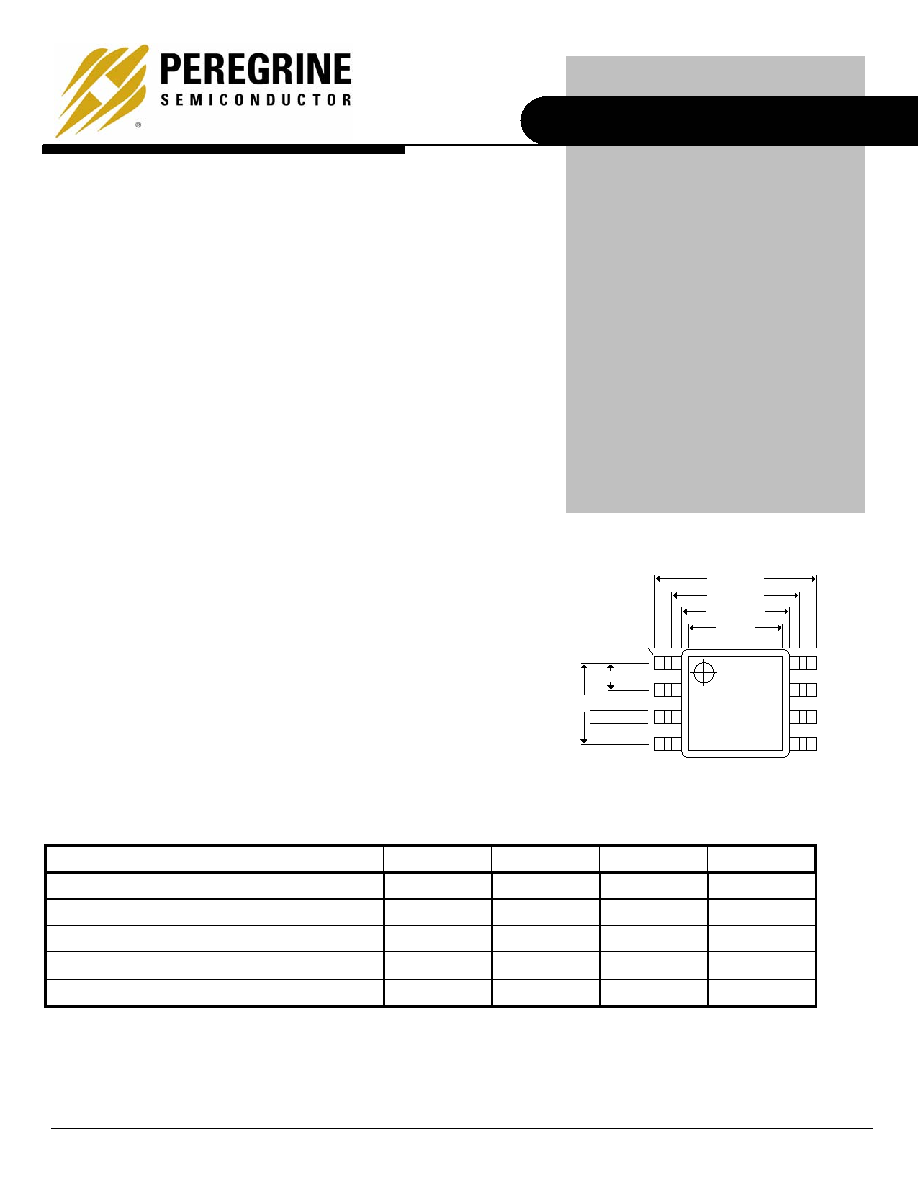
.220 / .250
.180 SQ Max
Pin 1
.166 SQ
.380 / .400
.150
.050 TYP
.015 .002 TYP
+-
Product Description
Product Benefits
� SEL Immune due to UTSi CMOS
� SEU <10
-10
errors / bit-day
� 100 Krads (Si) Total Dose
Figure 1. Package Drawings
Table 1. Electrical Specifications @ +25 �C
(Z
S
= Z
L
= 50
)
Parameter Minimum
Typical Maximum Units
Supply
Voltage
2.85 3.0 3.15 V
Supply Current
14
17
mA
Input Frequency (F
IN
) 1.5
3.5
GHz
Input Power (P
IN
) -10
+5
dBm
Output Power
-5
dBm
PRELIMINARY SPECIFICATION
PE9303
3.5 GHz Low Power CMOS
Divide-by-8 Prescaler For
RAD-Hard Applications
Features
� High-frequency operation:
1.5 GHz to 3.5 GHz
� Fixed divide ratio of 8
� Low-power operation: 14 mA
typical @ 3 V across frequency
� Small package: 8-lead formed
flat pack
The PE9303 is a high performance monolithic CMOS
prescaler with a fixed divide ratio of 8. Its operating
frequency range is 1.5 GHz to 3.5 GHz. The PE9303
operates on a nominal 3 V supply and draws only 14 mA.
It is packaged in a small 8-lead pre-formed flat pack and
is ideal for space applications.
The PE9303 is manufactured in Peregrine's patented
Ultra Thin Silicon (UTSi�) CMOS process, offering the
performance of GaAs with the economy and integration
of conventional CMOS.

PE9303
Preliiminary Specification
Copyright
Peregrine Semiconductor Corp. 2003
File No. 70/0052~01A
|
UTSi
CMOS RFIC SOLUTIONS
Page 2 of 6
Figure 2. Pin Configuration
Table 2. Pin Descriptions
Pin
No.
Pin
Name
Description
1
VDD
Power supply pin. Bypassing is required.
2
IN
Input signal pin. Should be coupled with a
capacitor (eg 15 pF).
3
DEC
Power supply decoupling pin. Place
capacitors as close as possible and
connect directly to the ground plane
(eg 10 nF & 10 pF).
4
GND
Ground pin. Ground pattern on the board
should be as wide as possible to reduce
ground impedance.
5 GND
Ground
pin.
6 GND
Ground
pin.
7
OUT
Divided frequency output pin. This pin
should be coupled with a capacitor
(eg 100 pF).
8 GND
Ground
Pin.
Table 3. Absolute Maximum Ratings
Symbol Parameter/Conditions Min Max Units
VDD Supply
voltage
4.0 V
T
ST
Storage
temperature
range
-65 150
�C
T
OP
Operating
temperature
range
-40 85
�C
VESD
ESD voltage (Human
Body Model)
250 V
P
INMAX
Maximum input power
10
dBm
Electrostatic Discharge (ESD) Precautions
When handling this UTSi device, observe the same
precautions that you would use with other ESD-
sensitive devices. Although this device contains
circuitry to protect it from damage due to ESD,
precautions should be taken to avoid exceeding the
rating specified in Table 3.
Latch-Up Avoidance
Unlike conventional CMOS devices, UTSi CMOS
devices are immune to latch-up.
Device Functional Considerations
The PE9303 takes an input signal frequency from
between 1.5 GHz to 3.5 GHz and produces an
output signal frequency one-fourth that of the
supplied input. In order for the prescaler to work
properly, several conditions need to be adhered to.
It is crucial that pin 3 be supplied with a bypass
capacitor to ground. In addition, the input and
output signals (pins 2 & 7, respectively) need to be
ac coupled via an external capacitor as shown in
the test circuit below.
The ground pattern on the board should be made
as wide as possible to minimize ground
impedance.
PE9303
1
2
3
4
8
7
6
5
IN
GND
DEC
GND
OUT
VDD
GND
GND

PE9303
Preliminary Specification
PEREGRINE SEMICONDUCTOR CORP.
|
http://www.peregrine-semi.com
Copyright
Peregrine Semiconductor Corp. 2003
Page 3 of 6
Figure 3. Test Circuit Block Diagram
Figure 4. High Frequency System Application
The wideband frequency of operation of the PE9303 makes it an ideal part for use in a DBS down converter
system.
BPF
SAW
AGC
FM
DEMOD
PE9303
PE9701
LOW NOISE
PLL SYNTH
LPF
BASEBAND
OUTPUT
DIVIDE BY 8
INPUT
DBS 1
st
IF
PE9303
1
2
3
4
5
6
7
8
DC
AC
Signal Generator
Spectrum Analyzer
50 Ohm
50 Ohm
100 pF
15 pF
10 nF
10 pF
1 nF
10 pF
VDD
3 V +/- 0.15 V
PE9303
Preliiminary Specification
Copyright
Peregrine Semiconductor Corp. 2003
File No. 70/0052~01A
|
UTSi
CMOS RFIC SOLUTIONS
Page 4 of 6
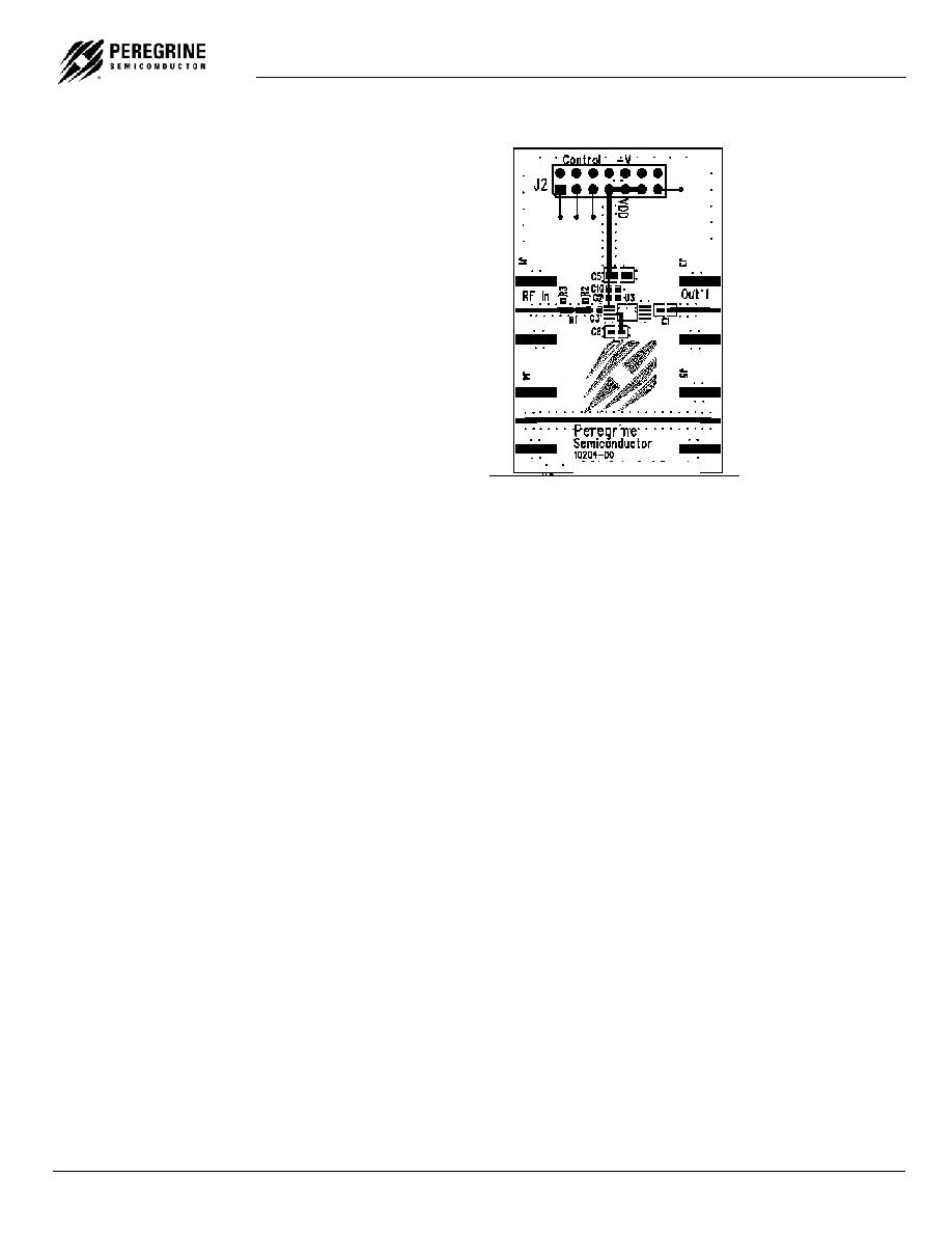
Evaluation Board Description
The PE9303 evaluation board is depicted in Figure
5. The input is driven into the RF In port while the
divided output is taken at Out 1. Both input and
output contain footprints for AC coupling capacitors
(C3 and C1 respectively). The power supply
connection is provided near the top of the
evaluation board, J2 Pin 1 as supply, J2 Pin 2 as
ground. In addition C2, C5, and C10 are
placeholders for power supply decoupling
capacitors. Placeholders C4, C6, and C8 are
needed for required bypass capacitors.
Note: C4 and C6 are located on the underside
of the evaluation board.
Figure 5. PE9303 Evaluation Board
Evaluation Board Test Setup
The PE9303 can be tested on the evaluation board
using the test setup shown in Figure 3 on page 3.
In the test setup, it is essential that the power
supply is properly decoupled and bypass
capacitors are used for pin 3. In addition, the input
and output need to be AC coupled.
Testing
The PE9303 Evaluation Board was measured prior
to shipment using the setup depicted in Figure 3.
Testing was performed at room temperature and
V
DD
= 2.85 V.
The input sensitivity plot for the PE9303 board is
included with the evaluation kit.
Applications Support
If you have a problem with your evaluation kit or if
you have applications questions call (858) 455-0660
and ask for applications support. You may also
contact us by fax or e-mail:
Fax: (858) 455-0770
E-Mail: help@peregrine-semi.com

PE9303
Preliminary Specification
PEREGRINE SEMICONDUCTOR CORP.
|
http://www.peregrine-semi.com
Copyright
Peregrine Semiconductor Corp. 2003
Page 5 of 6
Table 4. Ordering Information
Order
Code
Part Marking
Description
Package
Shipping
Method
9303-01
9303
PE9303-08CFPJ-B Engineering Samples
8-lead FLAT PACK
50 / Tray
9303-11
9303
PE9303-08CFPJ-B Production Units
8-lead FLAT PACK
50 / Tray
9303-00
PE9303-EK
PE9302 Evaluation Kit
Evaluation Board
1 / Box