 | –≠–ª–µ–∫—Ç—Ä–æ–Ω–Ω—ã–π –∫–æ–º–ø–æ–Ω–µ–Ω—Ç: 9312-11 | –°–∫–∞—á–∞—Ç—å:  PDF PDF  ZIP ZIP |

Page 1 of 7
Document No. 70-0119-02
www.psemi.com
©2005 Peregrine Semiconductor Corp. All rights reserved.
The PE9312 is a high-performance static UltraCMOSTM
prescaler with a fixed divide ratio of 4. Its operating frequency
range is DC to 1500 MHz. The PE9312 operates on a nominal
3 V supply and draws only 6.5 mA. It is packaged in a small
8-lead ceramic SOIC and is ideal for frequency scaling and
clock generation solutions.
The PE9312 is manufactured in Peregrine's patented Ultra-
Thin Silicon (UTSi
Æ
) CMOS process, offering the performance
of GaAs with the economy and integration of conventional
CMOS.
Product Description
Figure 1. Functional Diagram
Features
∑
DC to 1500 MHz operation
∑
Fixed divide ratio of 4
∑
Low-power operation: 6.5 mA typical
@ 3 V
∑
Ultra small package: 8-lead Ceramic
SOIC
∑
Guaranteed 100 Krads(Si) Total Dose
Performance
∑
Superior Single Event Upset Immunity
Table 1. Electrical Specifications @ +25 ∞C, V
DD
= 2.6 V
(Z
S
= Z
L
= 50
)
Parameter Conditions
Minimum
Typical
Maximum
Units
Supply Voltage
2.85
3.0
3.15
V
Supply Current
6.5
11
mA
Input Frequency (F
in
)
DC
1500
MHz
Input Power (P
in
)
DC <
Fin
∑
1000 MHz
-8
+10
dBm
1000 <
Fin
∑
1500 MHz
0
+10
dBm
Output Power (P
out
)
DC < Fin
∑
1500 MHz
0
dBm
V
DD
= 3.0 V, -40∞ C
T
A
85∞ C,
unless otherwise specified
D
QB
Q
CLK
D
QB
Q
CLK
Pre-Amp
Output
Buffer
IN
OUT
Product Specification
PE9312
1500 MHz Low Power UltraCMOSTM
Divide-by-4 Prescaler
Rad hard for Space Applications
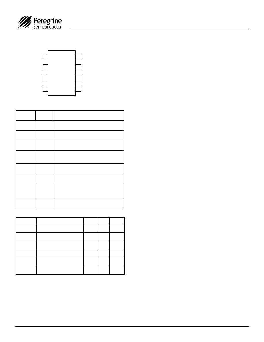
Figure 2. Package Type
8-lead CSOIC
Product Specification
PE9312
Page 2 of 7
©2005 Peregrine Semiconductor Corp. All rights reserved.
Document No. 70-0119-02
UltraCMOSTM RFIC Solutions
Table 2. Pin Descriptions
Table 3. Absolute Maximum Ratings
Device Functional Considerations
The PE9312 divides an input signal, up to a
frequency of 1500 MHz, by a factor of four thereby
producing an output frequency at a quarter of the
input frequency. To work properly at higher
frequency, the input and output signals (pins 2 &
7) must be AC coupled via an external capacitor,
as shown in the test circuit in Figure 8. The input
may be DC coupled for low frequency operation
with care taken to remain within the specified DC
input range for the device.
The ground pattern on the board should be made
as wide as possible to minimize ground
impedance. See Figure 7 for a layout example.
Latch-Up Avoidance
Unlike conventional CMOS devices, UltraCMOSTM
devices are immune to latch-up.
Figure 3. Pin Configuration
Electrostatic Discharge (ESD) Precautions
When handling this UltraCMOSTM device, observe
the same precautions that you would use with
other ESD-sensitive devices. Although this device
contains circuitry to protect it from damage due to
ESD, precautions should be taken to avoid
exceeding the rating specified in Table 3.
PE9312
1
2
3
4
8
7
6
5
IN
GND
N/C
GND
OUT
V
DD
NC
GND
Pin No.
Pin
Name
Description
1 V
DD
Power supply pin. Bypassing is required
(eg 1000 pF & 100 pF).
2 IN
Input signal pin. Should be coupled with a
capacitor (eg 1000 pF).
3 NC
No connection. This pin should be left
open.
4 GND
Ground pin. Ground pattern on the board
should be as wide as possible to reduce
ground impedance.
5 GND
Ground
pin.
6 NC
No connection. This pin should be left
open.
7 OUT
Divided frequency output pin. This pin
should be coupled with a capacitor
(eg 1000 pF).
8 GND
Ground
Pin.
Symbol Parameter/Conditions Min Max Units
V
DD
Supply voltage
4.0
V
P
in
Input
Power
15
dBm
V
IN
Voltage on input
-0.3
V
DD
+0.3
V
T
ST
Storage temperature range
-65
150
∞C
T
OP
Operating temperature
range
-40 85 ∞C
V
ESD
ESD voltage (Human Body
Model, MIL-STD 883)
1000
V
Absolute Maximum Ratings are those values
listed in the above table. Exceeding these values
may cause permanent device damage.
Functional operation should be restricted to the
limits in the DC Electrical Specifications table.
Exposure to absolute maximum ratings for
extended periods may affect device reliability.

Product Specification
PE9312
Page 3 of 7
Document No. 70-0119-02
www.psemi.com
©2005 Peregrine Semiconductor Corp. All rights reserved.
Typical Performance Data: V
DD
= 3.0 V
Figure 4. Input Sensitivity
Figure 5. Device Current
Figure 6. Output Power

Product Specification
PE9312
Page 4 of 7
©2005 Peregrine Semiconductor Corp. All rights reserved.
Document No. 70-0119-02
UltraCMOSTM RFIC Solutions
Figure 7. Test Circuit Block Diagram
50
VDD
IN
N/C
GND
GND
OUT
N/C
GND
1000 pF
100 pF
1000pF
1000pF
3 V
Power Meter or
Frequency Counter
50

Product Specification
PE9312
Page 5 of 7
Document No. 70-0119-02
www.psemi.com
©2005 Peregrine Semiconductor Corp. All rights reserved.
Evaluation Kit Operation
The Ceramic SOIC Prescaler Evaluation Board was
designed to help customers evaluate the PE9312
divide-by-2 prescaler. On this board, the device
input (pin 2) is connected to the SMA connector J1
through a 50
transmission line. A series capacitor
(C3) provides the necessary DC block for the device
input. A value of 1000 pF was used for the
evaluation board; other applications may require a
different value. It is also possible to place a 0
resistor in this location for very low frequency
applications.
The device output (pin 7) is connected to SMA
connector J3 through a 50
transmission line. A
series capacitor (C1) provides the necessary DC
block for the device output. This capacitor value
must be chosen to have a low impedance at the
desired output frequency of the device. A value of
1000 pF was chosen for the evaluation board.
The board is constructed of a two-layer FR4 material
with a total thickness of 0.031". The bottom layer
provides ground for the RF
transmission lines. The
transmission lines were designed using a coplanar
waveguide above ground plane model with trace
width of 0.030", trace gaps of 0.0061", dielectric
thickness of 0.028", metal thickness of 0.0014", and
r
of 4.6. Note that the predominate mode of these
transmission lines is coplanar waveguide.
J2 provides DC power to the device via pin 1. Two
decoupling capacitors (C2=100 pF, C10=1000 pF)
are included on this trace. It is the responsibility of
the customer to determine proper supply decoupling
for their design application.
Figure 8. Evaluation Board Layout
Figure 9. Evaluation Board Schematic
Peregrine specification 102/0202
Peregrine specification 102/0034