 | –≠–ª–µ–∫—Ç—Ä–æ–Ω–Ω—ã–π –∫–æ–º–ø–æ–Ω–µ–Ω—Ç: 94302-01 | –°–∫–∞—á–∞—Ç—å:  PDF PDF  ZIP ZIP |
Page 1 of 5
Document No. 70/0186-01
www.psemi.com
©2005 Peregrine Semiconductor Corp. All rights reserved.
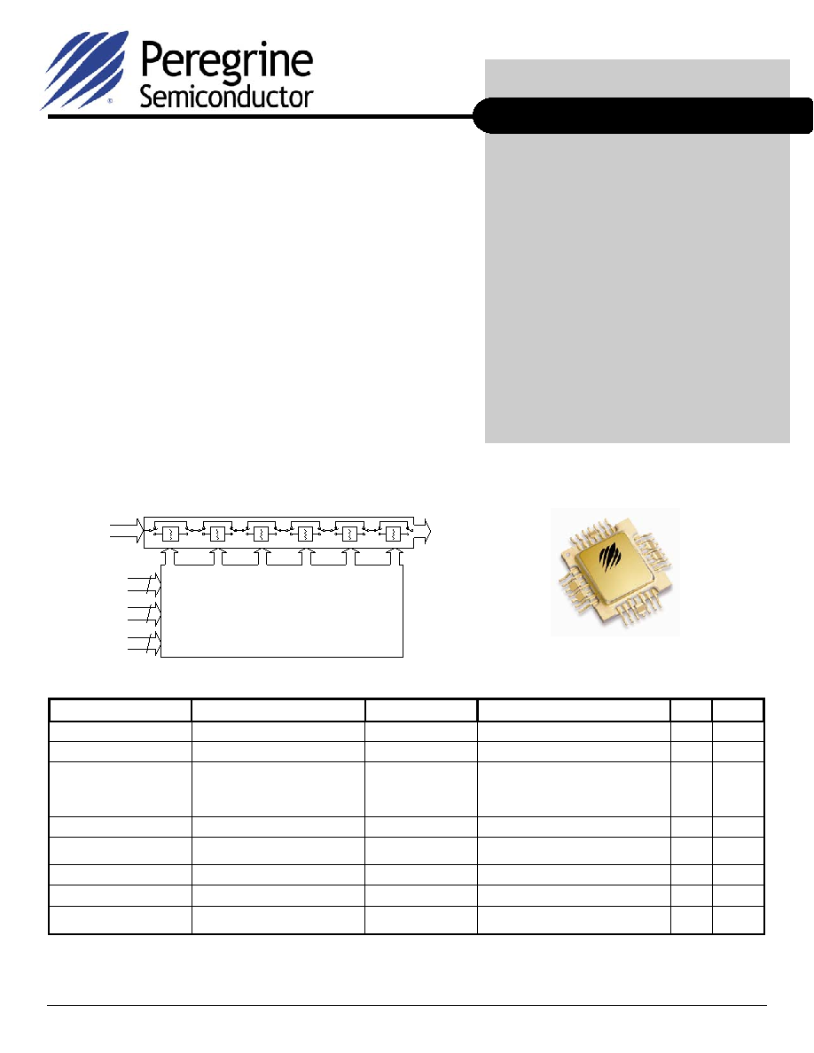
28-lead CQFP
Figure 2. Package Type
The PE94302 is a high linearity, 6-bit
UltraCMOS
TM
RF
Digital
Step Attenuator (DSA) specifically optimized for rad-hard space
applications. This 50-ohm RF DSA covers a 31.5 dB
attenuation range in 0.5 dB steps. It provides both parallel and
serial CMOS control interface which operate on a single 3-volt
supply. It also has a unique control interface that allows the
user to select an initial attenuation state at power-up. The PE
94302 maintains high attenuation accuracy over frequency and
temperature and exhibits very low insertion loss and power
consumption.
The PE94302 is manufactured in Peregrine's patented Ultra
Thin Silicon (UTSiÆ) CMOS process, offering the performance
of GaAs with the economy and integration of conventional
CMOS
.
Advance Information
50
RF Digital Step Attenuator
For Rad-Hard Space Applications
6-bit, 31.5 dB, DC ≠ 4.0 GHz
Product Description
Figure 1. Functional Schematic Diagram
PE94302
Features
∑
Attenuation: 0.5 dB steps to 31.5 dB
∑
Flexible parallel and serial programming
interfaces
∑
Unique power-up state selection
∑
Positive CMOS control logic
∑
High attenuation accuracy and linearity
over temperature and frequency
∑
Very low power consumption
∑
Single-supply operation
∑
50
impedance
Control Logic Interface
Parallel Control
Power-Up Control
Serial Control
RF Input
RF Output
Switched Attenuator Array
6
3
2
Table 1. Electrical Specifications @ +25∞C, V
DD
= 3.0 V
Parameter Test
Conditions
Frequency
Typical
Units
Operation Frequency
3
DC-4000
MHz
Insertion Loss
DC - 2.2 GHz
1.5
dB
Attenuation Accuracy
Any Bit or Bit Combination
0.5 dB - 23.5 dB Attenuation
24 dB - 31.5 dB Attenuation
DC
1.0 GHz
1.0 GHz
2.2 GHz
1.0 GHz
2.2 GHz
+/-(0.25 + 3% of attenuation setting)
+/-(0.25 + 5% of attenuation setting)
+/-(11% of attenuation setting)
dB
1 dB Compression
1,2
1 MHz - 2.2 GHz
34
dBm
Input IP3
1
Two-tone inputs
1 MHz - 2.2 GHz
52
dBm
Return Loss
DC - 2.2 GHz
20
dB
Switching Speed
50% control to 0.5 dB of final
value
1
µ
s
RF Input Power (50
)
dBm
Max
12
Notes: 1. Device Linearity will begin to degrade below 1 MHz
2. Maximum Operating Power = +12 dBm
3. Specs are guaranteed to 2.2 GHz, Characterized to 4.0 GHz

Advance Information
PE94302
Page 2 of 5
©2005 Peregrine Semiconductor Corp. All rights reserved.
Document No. 70/0186-01
UltraCMOSTM RFIC Solutions
Table 2. Pin Descriptions
Table 3. Absolute Maximum Ratings
Electrostatic Discharge (ESD) Precautions
When handling this UltraCMOSTM device, observe
the same precautions that you would use with
other ESD-sensitive devices. Although this device
contains circuitry to protect it from damage due to
ESD, precautions should be taken to avoid
exceeding the rate specified in Table 3.
Exposed Solder Pad Connection
The exposed solder pad on the bottom of the
package must be grounded for proper device
operation.
Table 4. DC Electrical Specifications
Figure 3. Pin Configuration (Top View)
Symbol Parameter/Conditions Min Max Units
V
DD
Power
supply
voltage
-0.3
4.0 V
V
I
Voltage on any input
-0.3
V
DD
+ V
T
ST
Storage temperature range
-65
150
∞C
P
IN
Input power (50
)
24
dBm
V
ESD
ESD voltage (Human Body
500
V
Parameter Min
Typ
Max
Units
V
DD
Power Supply
Voltage
2.7 3.0 3.3 V
I
DD
Power Supply
Current
100
µ
A
Digital Input High
0.7xV
DD
V
Digital Input Low
0.3xV
DD
V
Digital Input Leakage
1
µ
A
T
OP
Operating
-40
85
∞C
Latch-Up Avoidance
Unlike conventional CMOS devices, UltraCMOSTM
devices are immune to latch-up.
Switching Frequency
The PE94302 has a maximum 25 kHz switching
rate.
Pin No.
Pin Name
1 C16
2 GND
3 RF1
4 GND
5 Data
6 GND
7 CLK
8 LE
9 V
DD
10 GND
11 PUP1
12 GND
13 PUP2
14 V
SS
15 POR
16 GND
17 P/S
18 GND
19 RF2
20 GND
21 C8
22 C4
23 C2
24 GND
25 GND
26 GND
27 C1
28 C0.5
Paddle GND
Description
Attenuation control bit, 16dB
Ground connection
RF port (Note 1).
Ground connection
Serial interface data input
Ground connection
Serial interface clock input.
Latch Enable input (Note 2).
Power supply pin.
Ground connection
Power-up selection bit, MSB.
Ground connection
Power-up selection bit, LSB.
Negative supply voltage
Power reset
Ground connection
Parallel/Serial mode select.
Ground connection
RF port (Note 1).
Ground connection
Attenuation control bit, 8 dB.
Attenuation control bit, 4 dB.
Attenuation control bit, 2 dB.
Ground connection
Ground connection
Ground connection
Attenuation control bit, 1 dB.
Attenuation control bit, 0.5 dB.
Ground connection
PE94302
25
11
5
3
17
19
1
2
4
18
6
7
20
21
16
15
26
24
27
28
23
22
10
9
8
12
13
14
C16
GND
RF1
GND
GND
GND
GND
GND
GND
GND
GND
GND
GND
Data
CLK
LE
V
DD
PUP1
PUP2
V
SS
POR
P/S
RF2
C8
C4
C2
C1
C0
.
5
Note 1: Both RF ports must be held at 0 V
DC
or DC blocked with an
external series capacitor.
2: Latch Enable (LE) has an internal 100 k resistor to V
DD.
Absolute Maximum Ratings are those values
listed in the above table. Exceeding these values
may cause permanent device damage.
Functional operation should be restricted to the
limits in the DC Electrical Specifications table.
Exposure to absolute maximum ratings for
extended periods may affect device reliability.

Advance Information
PE94302
Page 3 of 5
Document No. 70/0186-01
www.psemi.com
©2005 Peregrine Semiconductor Corp. All rights reserved.
-5
-4
-3
-2
-1
0
1
0
8
16
24
32
Attenuation Setting (dB)
Erro
r (
d
B
)
250 M Hz
500 M Hz
1000 M Hz
1500 M Hz
2000 M Hz
-5
-4
-3
-2
-1
0
0
500
1000
1500
2000
RF Frequency (MHz)
I
n
s
e
r
t
i
o
n Los
s
(d
B
)
Mean insertion loss
Typical Performance Data (25∞C, V
DD
=3.0 V)
Figure 5. Attenuation Error Vs. Attenuation
Setting
Figure 4. Insertion Loss Vs. Frequency

Advance Information
PE94302
Page 4 of 5
©2005 Peregrine Semiconductor Corp. All rights reserved.
Document No. 70/0186-01
UltraCMOSTM RFIC Solutions
Table 10. Ordering Information
Order Code
Part Marking
Description
Package
Shipping
Method
94302-01
94302
PE94302-28CQFP-50B Engineering Samples
28-lead CQFP
50 Count Trays
94302-11
94302
PE94302-28CQFP-50B Production Units
28-lead CQFP
50 Count Trays
94302-00
PE94302-EK
PE94302 Evaluation Kit
Evaluation Board
1 / Box
Figure 6. Package Drawing
28-lead CQFP
NOTES:
1.
METALLIZATION/ PLATING: REFRACTORY METAL = Ni (75~350u") = Au (50u"MIN)
2. METALLIZED
CASTELLATIONS.
3.
DIELECTIC RUN INTO CASTELLATIONS SHALL BE ACCEPTABLE.
4.
GOLD SPECKLES ON DIELECTRIC COAT SHALL BE ACCEPTABLE.
5.
VISUAL ANOMALIES IN CASTELLATION METALLIZATION ACCEPTABLE.
6.
TEXT AND ITS LOCATIONS ON LEAD FRAME ARE VENDOR'S OPTION.
7.
SLIGHT PATTERN MISMATCH WITH DRAWING DUE TO DIELECTRIC COAT MISALIGNMENT SHALL BE ACCEPTABLE.
8.
SEAL RING & HEAT SINK ARE CONNECTED TO GND.
9.
LEAD INTEGRITY (ADHESION/ ALIGNMENT/ COPRANARITY), CASTELLATION QUALITY ARE BEST EFFORT BASIS.

Advance Information
PE94302
Page 5 of 5
Document No. 70/0186-01
www.psemi.com
©2005 Peregrine Semiconductor Corp. All rights reserved.
Sales Offices
The Americas
Peregrine Semiconductor Corp.
9450 Carroll Park Drive
San Diego, CA 92121
Tel 858-731-9400
Fax 858-731-9499
North Asia Pacific
Peregrine Semiconductor K.K.
5A-5, 5F Imperial Tower
1-1-1 Uchisaiwaicho, Chiyoda-ku
Tokyo 100-0011 Japan
Tel: +81-3-3502-5211
Fax: +81-3-3502-5213
Europe
Peregrine Semiconductor Europe
Commercial Products:
B‚timent Maine
13-15 rue des Quatre Vents
F- 92380 Garches, France
Tel: +33-1-47-41-91-73
Fax : +33-1-47-41-91-73
Space and Defense Products:
180 Rue Jean de Guiramand
13852 Aix-En-Provence cedex 3, France
Tel: +33(0) 4 4239 3361
Fax: +33(0) 4 4239 7227
For a list of representatives in your area, please refer to our Web site at: www.psemi.com
Data Sheet Identification
Advance Information
The product is in a formative or design stage. The data
sheet contains design target specifications for product
development. Specifications and features may change in
any manner without notice.
Preliminary Specification
The data sheet contains preliminary data. Additional data
may be added at a later date. Peregrine reserves the right
to change specifications at any time without notice in order
to supply the best possible product.
Product Specification
The data sheet contains final data. In the event Peregrine
decides to change the specifications, Peregrine will notify
customers of the intended changes by issuing a DCN
(Document Change Notice).
The information in this data sheet is believed to be reliable.
However, Peregrine assumes no liability for the use of this
information. Use shall be entirely at the user's own risk.
No patent rights or licenses to any circuits described in this
data sheet are implied or granted to any third party.
Peregrine's products are not designed or intended for use in
devices or systems intended for surgical implant, or in other
applications intended to support or sustain life, or in any
application in which the failure of the Peregrine product could
create a situation in which personal injury or death might occur.
Peregrine assumes no liability for damages, including
consequential or incidental damages, arising out of the use of
its products in such applications.
The Peregrine name, logo, and UTSi are registered trademarks
and UltraCMOS is a trademark of Peregrine Semiconductor
Corp.
South Asia Pacific
Peregrine Semiconductor
28G, Times Square,
No. 500 Zhangyang Road,
Shanghai, 200122, P.R. China
Tel: +86-21-5836-8276
Fax: +86-21-5836-7652