 | –≠–ª–µ–∫—Ç—Ä–æ–Ω–Ω—ã–π –∫–æ–º–ø–æ–Ω–µ–Ω—Ç: 9704-01 | –°–∫–∞—á–∞—Ç—å:  PDF PDF  ZIP ZIP |

PEREGRINE SEMICONDUCTOR CORP.
|
http://www.peregrine-semi.com
Copyright
Peregrine Semiconductor Corp. 2003
Page 1 of 12
Product Description
Figure 1. Block Diagram
ADVANCE INFORMATION
PE9704
3.0 GHz Integer-N PLL for Rad
Hard Applications
Features
∑ 3.0 GHz operation
∑ ˜10/11 dual modulus prescaler
∑ Phase detector output
∑ Serial interface or hardwired
programmable
∑ Ultra-low phase noise
∑ SEU < 10
-9
errors / bit-day
∑ 100 Krad (Si) total dose
∑ 44-lead CQFJ
Peregrine's PE9704 is a high-performance integer-N PLL
capable of frequency synthesis up to 3.0 GHz. The
device is designed for superior phase noise performance
while providing an order of magnitude reduction in
current consumption, when compared with existing
commercial space PLLs.
The PE9704 features a ˜10/11 dual modulus prescaler,
counters, and a phase comparator as shown in Figure 1.
Counter values are programmable through a serial
interface, and can also be directly hard wired.
The PE9704 is optimized for commercial space
applications. Single Event Latch-up (SEL) is physically
impossible and Single Event Upset (SEU) is better than
10
-9
errors per bit / day. Fabricated in Peregrine's
patented UTSiÆ (Ultra Thin Silicon) CMOS technology,
the PE9704 offers excellent RF performance and intrinsic
radiation tolerance.
F
IN
Prescaler
10 / 11
Main
Counter
20-Bit
Frequency
Register
M(8:0)
A(3:0)
R(5:0)
19*
20
R Counter
F
R
Phase
Detector
6
6
13
Serial
Control
PD_U
PD_D
3
MSEL
f
p
f
c
Direct
Control
* prescaler bypass not available in Direct mode
LD
C ext

PE9704
Advance Information
Copyright
Peregrine Semiconductor Corp. 2003
File No. 70/0083~00B
|
|
UTSi CMOS RFIC SOLUTIONS
Page 2 of 12
11
12
13
14
15
16
17
10
9
8
7
6
5
4
3
2
1 44 43 42 41 40
35
34
33
32
31
30
29
36
37
38
39
18 19 20 21 22 23 24 25 26 27 28
R
4
R
5
M
0
M
1
V
DD
V
DD
M
2
M
3
S_WR, M
4
DATA, M
5
GND
GND
N/C
V
DD
D
OUT
V
DD
N/C
GND
PD_D
PD_U
V
DD
CLO
C
K
,
M
6
GN
D
R
3
R
2
R
1
R
0
V
DD
LD
ENH
F
R
GN
D
GN
D
C
EXT
M
7
M
8
A
0
D
MO
DE
V
DD
E_
WR
,
A
1
A
2
A
3
F
IN
GN
D
Figure 2. Pin Configuration
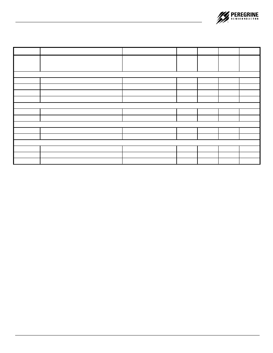
Table 1. Pin Descriptions
Pin No.
Pin Name
Interface Mode
Type
Description
1 V
DD
Both
(Note
1)
Power supply input. Input may range from 2.85 V to 3.15 V. Bypassing
recommended.
2 R
0
Direct
Input
R Counter bit0
3 R
1
Direct
Input
R Counter bit1
4 R
2
Direct
Input
R Counter bit2
5 R
3
Direct
Input
R Counter bit3
6 GND Both
(Note
1)
Ground
7 R
4
Direct
Input
R Counter bit4
8 R
5
Direct
Input
R Counter bit5 (MSB)
9 M
0
Direct
Input
M
Counter
bit0
10 M
1
Direct
Input
M
Counter
bit1
11 V
DD
Both
(Note 1)
Same as pin 1
12 V
DD
Both
(Note 1)
Same as pin 1
13 M
2
Direct
Input
M
Counter
bit2
14 M
3
Direct
Input
M
Counter
bit3
S_WR Serial
Input
Frequency register load enable input. Buffered data is transferred to the frequency
register on S_WR rising edge.
15
M
4
Direct
Input
M
Counter
bit4
16
DATA Serial
Input
Binary serial data input. Data is entered LSB first, and is clocked serially into the 20-
bit frequency control register (E_WR "low") or the 8-bit enhancement register (E_WR
"high") on the rising edge of CLOCK.

PE9704
Advance Information
PEREGRINE SEMICONDUCTOR CORP.
|
http://www.peregrine-semi.com
Copyright
Peregrine Semiconductor Corp. 2003
Page 3 of 12
Pin No.
Pin Name
Interface Mode
Type
Description
M
5
Direct
Input
M
Counter
bit5
17 GND Both
Ground
CLOCK Serial
Input
Clock input. Data is clocked serially into either the 20-bit primary register (E_WR
"low") or the 8-bit enhancement register (E_WR "high") on the rising edge of CLOCK.
18
M
6
Direct
Input
M
Counter
bit6
19 M
7
Direct
Input
M
Counter
bit7
20 M
8
Direct
Input
M Counter bit8 (MSB)
21 A
0
Direct
Input
A Counter bit0
22 D
MODE
Both
Input
Selects direct interface mode (D
MODE
=1) or serial interface mode (D
MODE
=0)
23 V
DD
Both
(Note 1)
Same as pin 1
E_WR Serial
Input
Enhancement register write enable. While E_WR is "high", DATA can be serially
clocked into the enhancement register on the rising edge of CLOCK.
24
A
1
Direct
Input
A Counter bit1.
25 A
2
Direct
Input
A Counter bit2
26 A
3
Direct
Input
A Counter bit3 (MSB)
27 F
IN
Both
Input
RF prescaler input from the VCO. 3.0 GHz maximum frequency.
28 GND Both
Ground.
29 GND Both
Ground.
30 N/C
No
connect.
31 V
DD
Both
(Note 1)
Same as pin 1
32 D
OUT
Serial
Output
Data Out. The Main Counter output, R Counter output, or dual modulus prescaler
select (MSEL) can be routed to D
OUT
through enhancement register programming.
33 V
DD
Both
(Note 1)
Same as pin 1
34 N/C
No
connect.
35 GND Both
Ground.
36 PD_D Both
Output
PD_D pulses down when f
p
leads f
c
.
37 PD_U Both
PD_U pulses down when f
c
leads f
p
.
38 V
DD
Both
(Note 1)
Same as pin 1
39 C
EXT
Both
Output
Logical "NAND" of PD_U and PD_D, passed through an on-chip, 2 k
series resistor.
Connecting C
EXT
to an external capacitor will low pass filter the input to the inverting
amplifier used for driving LD.
40 GND Both
Ground
41 GND Both
Ground
42 F
R
Both
Input
Reference frequency input
43
ENH
Both Output,
OD
Enhancement mode. When asserted low ("0"), enhancement register bits are
functional.
44 LD
Serial Output
Lock detect output, the open-drain logical inversion of C
EXT
. When the loop is locked,
LD is high impedance; otherwise LD is a logic low ("0").
Note 1: V
DD
pins 1, 11, 12, 23, 31, 33, 35, and 38 are connected by diodes and must be supplied with the same positive voltage level.
Note 2: All digital input pins have 70 k
pull-down resistors to ground.

PE9704
Advance Information
Copyright
Peregrine Semiconductor Corp. 2003
File No. 70/0083~00B
|
|
UTSi CMOS RFIC SOLUTIONS
Page 4 of 12
Table 2. Absolute Maximum Ratings
Symbol Parameter/Conditions Min Max Units
V
DD
Supply
voltage
-0.3
4.0 V
V
I
Voltage on any input
-0.3
V
DD
+ 0.3
V
I
I
DC into any input
-10
+10
mA
I
O
DC into any output
-10
+10
mA
T
stg
Storage
temperature
range
-65 150
∞C
Table 3. Operating Ratings
Symbol Parameter/Conditions Min Max Units
V
DD
Supply
voltage
2.85
3.15 V
T
A
Operating
ambient
temperature range
-40 85
∞C
Table 4. ESD Ratings
Symbol Parameter/Conditions Level
Units
V
ESD
ESD voltage (Human Body
Model) ≠ Note 1
1000 V
Note 1: Periodically sampled, not 100% tested. Tested per MIL-
STD-883, M3015 C2
Electrostatic Discharge (ESD) Precautions
When handling this UTSi device, observe the same
precautions that you would use with other ESD-
sensitive devices. Although this device contains
circuitry to protect it from damage due to ESD,
precautions should be taken to avoid exceeding the
rating specified in Table 4.
Latch-Up Avoidance
Unlike conventional CMOS devices, UTSi CMOS
devices are immune to latch-up.
PE9704
Advance Information
PEREGRINE SEMICONDUCTOR CORP.
|
http://www.peregrine-semi.com
Copyright
Peregrine Semiconductor Corp. 2003
Page 5 of 12
Table 5. DC Characteristics
V
DD
= 3.0 V, -40
∞ C < T
A
< 85
∞ C, unless otherwise specified
Symbol Parameter
Conditions
Min
Typ
Max
Units
I
DD
Operational supply current;
Prescaler disabled
Prescaler enabled
V
DD
= 2.85 to 3.15 V
10
24
31
mA
mA
Digital Inputs: All except F
R
, F
IN
(all digital inputs have 70k ohm pull-up resistors)
V
IH
High level input voltage
V
DD
= 2.85 to 3.15 V
0.7 x V
DD
V
V
IL
Low level input voltage
V
DD
= 2.85 to 3.15 V
0.3 x V
DD
V
I
IH
High level input current
V
IH
= V
DD
= 3.15 V
+70
µA
I
IL
Low level input current
V
IL
= 0, V
DD
= 3.15 V
-1
µA
Reference Divider input: F
R
I
IHR
High level input current
V
IH
= V
DD
= 3.15 V
+100
µA
I
ILR
Low level input current
V
IL
= 0, V
DD
= 3.15 V
-100
µA
Counter and phase detector outputs: f
c
, f
p
.
V
OLD
Output voltage LOW
I
out
= 6 mA
0.4
V
V
OHD
Output
voltage
HIGH
I
out
= -3 mA
V
DD
- 0.4
V
Lock detect outputs: C
EXT
, LD
V
OLC
Output voltage LOW, C
EXT
I
out
= 100 µ
0.4
V
V
OHC
Output voltage HIGH, C
EXT
I
out
= -100 µ
V
DD
- 0.4
V
V
OLLD
Output voltage LOW, LD
I
out
= 6 mA
0.4
V