
PEREGRINE SEMICONDUCTOR CORP.
|
http://www.peregrine-semi.com
Copyright
Peregrine Semiconductor Corp. 2003
Page 1 of 7
Product Description
Product Benefits
∑ SEL Immune UTSi CMOS-on-sapphire
∑ SEU <10
-10
errors / bit-day
∑ 300 Krad Total Dose
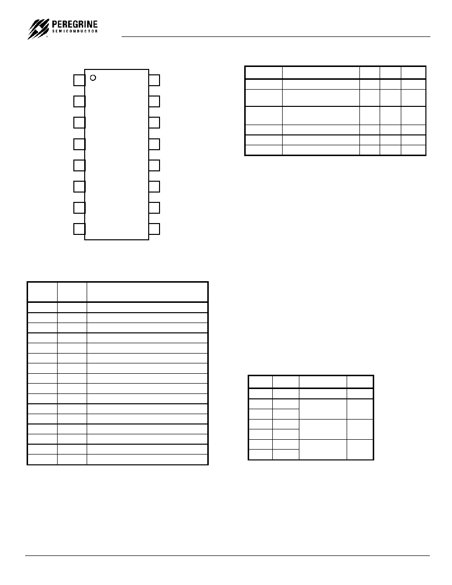
Figure 1. Package Drawing
ADVANCE INFORMATION
PE26C32
Quad RS-422 Differential Line
Receiver Radiation Hardened
Features
∑ High-speed operation: < 15 nS
typical
∑ Low power: < 9 mA typical
∑ 3.3 V operation
∑ Standard packaging: 16-lead
DIP and flat pack
The PE26C32 is a high performance monolithic CMOS
RS-422 line receiver. Its operating supply range is 3.0 to
3.6V, with an input signal common mode range of +/-
10V. The PE26C32 offers higher speed and lower power
than other RS-422 receiver types. It is packaged in
standard DIP and flat pack options and is ideal for space
applications.
The PE26C32 is manufactured in Peregrine's patented
Ultra Thin Silicon (UTSiÆ) CMOS process, offering the
performance of GaAs with the low power, economy and
integration of conventional CMOS.
PE26C32
Preliminary Specification
Copyright
Peregrine Semiconductor Corp. 2003
File No. 70/0101~00A
|
UTSi CMOS RFIC SOLUTIONS
Page 2 of 7
Figure 2. Pin Configuration
Table 1. Pin Descriptions
Pin
No.
Pin
Name
Description
1
A-
Channel A Inverting Input
2
A+
Channel A Noninverting Input
3
AQ
Channel A Output
4
E+
Enable, active high
5
BQ
Channel B Output
6
B+
Channel B Noninverting Input
7
B-
Channel B Inverting Input
8 V-
Ground
Pin
9
C-
Channel C Inverting Input
10
C+
Channel C Noninverting Input
11 CQ
Channel
C
Ouput
12
E-
Enable, active low
13 DQ
Channel
D
Output
14
D+
Channel D Noninverting Input
15
D-
Channel D Inverting Input
16 V+
Supply
Pin
Table 2. Recommended Operating Conditions
Symbol Parameter/Conditions Min Max Units
V+ Supply
voltage
3.0
3.6 V
T
OP
Operating
temperature
range
-55 125
∞C
VIN (Line)
Maximum input voltage
A+/-, B+/-, C+/-, D+/-
-7 7 V
VIN (Dig)
Maximum input voltage
0
(V+)
V
VOUT Maximum
output
voltage 0 (V+) V
IOUT Maximum
output
current -10 10 mA
Electrostatic Discharge (ESD) Precautions
When handling this UTSi device, observe the same
precautions that you would use with other ESD-
sensitive devices. Although this device contains
circuitry to protect it from damage due to ESD,
precautions should be taken to avoid exceeding the
rating specified in Table 2.
Latch-Up Avoidance
Unlike conventional CMOS devices, UTSi CMOS
devices are immune to latch-up.
Device Functional Considerations
The PE26C32 operates at high switching speeds.
In order to obtain maximum performance, it is
crucial that pin 16 be supplied with a bypass
capacitor to ground (pin 8).
Table 3. Truth Table
E+ E- Vin
(Diff) Q
L H
X
Z
H X
X L
<-200 mV
L
H X
X L
>+200 mV
H
H X
X L
Open H
1
A-
PE26C32
2
A+
3
AQ
4
E+
5
BQ
6
B+
7
B-
8
V-
16
15
14
13
12
11
10
9
V+
D-
D+
DQ
E-
CQ
C-
C+

PE26C32
Advance Information
PEREGRINE SEMICONDUCTOR CORP.
|
http://www.peregrine-semi.com
Copyright
Peregrine Semiconductor Corp. 2003
Page 3 of 7
Table 4. Electrical Specifications
-55∞ C < Tcase < 125∞ C, 3.0 V < V+ < 3.6 V, PreRad,
unless otherwise specified
Parameter Minimum
Typical Maximum Units
Supply Voltage
3.0 3.3 3.6 V
Supply Current (Line inputs open, enabled)
(V+)=3.3V
(V+)=5.5V
9
12
mA
mA
Input Threshold (Line, differential)
VCM=+7
VCM=0
VCM=-7
-200
-200
-200
200
200
200
mV
mV
mV
Input Threshold Hysteresis (Line, Differential)
VCM=0
5 30 100
mV
Input Resistance (Line pins)
VCM=+7
VCM=0
VCM=-7
10 K
10 K
10 K
25 K
25 K
25 K
Ohms
Ohms
Ohms
Input Threshold (Enable)
(V+)*0.3 (V+)/2 (V+)*0.7 V
Input Current (Enable)
-1 1 uA
Input "Failsafe" Open Circuit Differential voltage
200 500
mV
Output Drive Current @ 0.5 V from rail (high or low)
10 mA
Output Short Circuit Current (to V-)
15 75
mA
Output Tristate Current, 0 < Vout < V+
-5 5 uA
VOH @ 10 mA
(V+) ≠ 0.5 V
(V+) ≠ 0.4
(V+)
V
VOL @ 10 mA
0 0.4
0.5
V V
TPHL (See Fig 2)
12 20
nS
TPLH (See Fig 2)
12 20
nS
TPZL, TPZH (See Fig 3)
10 20
nS
TPHZ, TPLZ (See Fig 3)
10 30
nS
FMAX
50 MHz
Notes:
(1) "Line" pins refer to A-, A+, B-, B+, C-, C+, D-, D+, differential outputs
(2) "Digital Input" or "Enable" pins refer to E+, E-
(3) "Digital Input" pins refer to AQ, BQ, CQ, DQ
(4) Output Short Circuit not intended to imply continuous operation

PE26C32
Preliminary Specification
Copyright
Peregrine Semiconductor Corp. 2003
File No. 70/0101~00A
|
UTSi CMOS RFIC SOLUTIONS
Page 4 of 7
Table 5. Post-Irradiation DC Electrical Specifications
Tcase = 25∞ C, 3.0 V < V+ < 3.6 V, 300 KRad,
unless otherwise specified
Parameter Minimum
Typical Maximum Units
Supply Voltage
3.0 3.3 3.6 V
Supply Current (Line inputs open, enabled)
(V+)=3.3 V
(V+)=5.5 V
10
14
mA
mA
Input Threshold (Line, differential)
VCM=+7
VCM=0
VCM=-7
-200
-200
-200
200
200
200
mV
mV
mV
Input Threshold Hysteresis (Line, Differential)
VCM=0
5 30 100
mV
Input Resistance (Line pins)
VCM=+7
VCM=0
VCM=-7
10K
10K
10K
20K
20K
20K
Ohms
Ohms
Ohms
Input Threshold (Enable)
(V+)*0.3 (V+)/2 (V+)*0.7 V
Input Current (Enable)
-1 1 uA
Input "Failsafe" Open Circuit Differential voltage
200 500
mV
Output Drive Current @ 0.5 V from rail (high or low)
10 mA
Output Short Circuit Current (to V-)
15 75
mA
Output Tristate Current, 0 < Vout < V+
-10 10 uA
VOH @ 10 mA
(V+) ≠ 0.5 V
(V+) ≠ 0.4
(V+)
V
VOL @ 10 mA
0 0.4
0.5
V V
TPHL (See Fig 2)
15 25
nS
TPLH (See Fig 2)
15 25
nS
TPZL, TPZH (See Fig 3)
15 25
nS
TPHZ, TPLZ (See Fig 3)
15 30
nS
FMAX
50 MHz
Notes:
(1) "Line" pins refer to A-, A+, B-, B+, C-, C+, D-, D+, differential outputs
(2) "Digital Input" or "Enable" pins refer to E+, E-
(3) "Digital Input" pins refer to AQ, BQ, CQ, DQ
(4) Output Short Circuit not intended to imply continuous operation

PE26C32
Advance Information
PEREGRINE SEMICONDUCTOR CORP.
|
http://www.peregrine-semi.com
Copyright
Peregrine Semiconductor Corp. 2003
Page 5 of 7
Figure 3. TPLH, TPHL Test Circuit Block Diagram
Figure 4. TPLZ, TPZL, TPHZ, TPZH Test Circuit Block Diagram
VI-
1.0 ≠ 2.0
VI+
1.0 ≠ 2.0
+
-
CL
15pF
DC
2,6,10,14
1,7,9,15
3,5,11,13
4,16
8,12
Figure 2: TPLH, TPHL
TPLH, TPHL measured from input 50% to output
50% thresholds. TRISE, TFALL measured from
output 20% to output 80% thresholds.
I-
I+
Q
TPLH
TPLH
Q
TRISE
TFALL
VI-
VI+
L: 0.0
H: 1.5
+
-
CL
15pF
DC
2,6,10,14
1,7,9,15
3,5,11,13
16
Figure 3: TPHZ, TPZH, TPLZ, TPZL
RL
2K
DC
DC
L: 1.5
H: 0.0
Vcc
3.3V
E+/E-
0-(V+)
4
13
TPZH, TPZL measured from input 50% to output
50% thresholds. TPHZ, TPLZ measured from
input 50% to output 10% thresholds.
E-
E+
Q
TPZH
TPHZ
Q
TPLZ
TPZL