 | –≠–ª–µ–∫—Ç—Ä–æ–Ω–Ω—ã–π –∫–æ–º–ø–æ–Ω–µ–Ω—Ç: PE3293-15 | –°–∫–∞—á–∞—Ç—å:  PDF PDF  ZIP ZIP |
PEREGRINE SEMICONDUCTOR CORP.
|
http://www.peregrine-semi.com
Copyright
Peregrine Semiconductor Corp. 2003
Page 1 of 18
Product Description
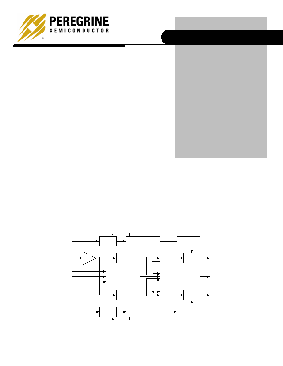
Figure 1. Block Diagram
PRODUCT SPECIFICATION
PE3293
1.8 GHz / 550 MHz Dual
Fractional-N Ultra-Low
Spurious PLL for Frequency
Synthesis
Features
∑ Industry leading fractional spur
compensation: no adjusting
required, stable over temp.
∑ Ultra-Low Power consumption:
4.0 mA typical, both loops
operating
∑ Modulo-32 fractional-N main
counters
∑ Supply voltage range 2.7 to 3.3
VDC
The PE3293 is a dual fractional-N phase-lock loop (PLL)
IC designed for frequency synthesis and fabricated on
Peregrine's patented UTSiÆ CMOS process. Each PLL
includes a prescaler, phase detector, charge pump and
on-board fractional spur compensation.
The patented spur compensation circuitry designed into
the device ensures superior spur performance over the
full temperature and VCO tuning range.
The PE3293 provides fractional-N division with power-of-
two denominator values up to 32. This allows
comparison frequencies up to 32 times the channel
spacing, providing a lower phase noise floor than integer
PLLs. The 32/33 RF prescaler (PLL1) operates up to 1.8
GHz and the 16/17 IF prescaler (PLL2) operates up to
550 MHz.
Applications
∑ Triple mode,dual-band PCS / Cellular handset
∑ PCS/CDMA/Cellular handsets
∑ PCS/CDMA/Cellular base stations
32/33
Prescaler
f
in
1
19-bit Fractional-N
Main Divider
Fractional Spur
Compensation
Fractional Spur
Compensation
18-bit Fractional-N
Main Divider
9-bit Reference
Divider
9-bit Reference
Divider
21-bit Serial Control
Interface
Ref.
Amp.
f
r
Clock
Data
LE
f
in
2
16/17
Prescaler
f
o
LD
CP1
CP2
Phase
Detector
Phase
Detector
Charge
Pump
Charge
Pump
Multiplexer
PE3293
Product Specification
Copyright
Peregrine Semiconductor Corp. 2003
File No. 70/0015~02C
|
UTSi CMOS RFIC SOLUTIONS
Page 2 of 18
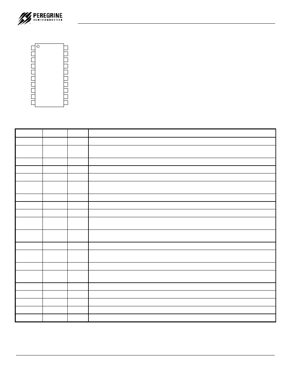
Figure 2. Pin Configuration: TSSOP (JEDEC MO-153-AC)
Table 1. Pin Descriptions
Pin No.
Pin Name
Type
Description
1
N / C
No connect.
2 V
DD
(Note
1)
Power supply voltage input. Input may range from 2.7 V to 3.3 V. A bypass capacitor should be placed as
close as possible to this pin and be connected directly to the ground plane.
3
CP1
Output
Internal charge-pump output from PLL1 for connection to a loop filter for driving the input of an external VCO.
4 GND
Ground.
5 f
in
1
Input
Prescaler input from the PLL1 (RF) VCO. Maximum frequency is 1.8 GHz.
6 Dec1
Power supply decoupling pin for PLL1. A capacitor should be placed as close as possible to this pin and be
connected directly to the ground plane.
7 V
DD1
PLL1 prescaler power supply. 3.3 kohm resistor to V
DD
.
8 f
r
Input
Reference frequency input.
9 GND
Ground.
10 f
o
LD Output
Multiplexed output of the PLL1 and PLL2 main counters or reference counters, Lock Detect signals, and data
out of the shift register. CMOS output (see Table 11, f
o
LD Programming Truth Table).
11 Clock
Input
CMOS clock input. Serial data for the various counters is clocked in on the rising edge into the 21-bit shift
register.
12
Data
Input
Binary serial data input. CMOS input data entered MSB first. The two LSBs are the control bits.
13 LE
Input
Load Enable CMOS input. When LE is high, data word stored in the 21-bit serial shift register is loaded into
one of the four appropriate latches (as assigned by the control bits).
14 V
DD2
Output
PLL2 prescaler power supply. 3.3 kohm resistor to V
DD
.
15 Dec2
Output
Power supply decoupling pin for PLL2. A capacitor should be placed as close as possible to this pin and be
connected directly to the ground plane.
16 f
in
2
Input
Prescaler input from the PLL2 (IF) VCO. Maximum frequency is 550 MHz.
17 GND
Ground.
18
CP2
Output
Internal charge-pump output for PLL2. For connection to a loop filter for driving the input of an external VCO.
19 V
DD
(Note 1)
Same as pin 2.
20 V
DD
(Note 1)
Same as pin 2.
Note 1: V
DD
pins 2, 19, and 20 are connected by diodes and must be supplied with the same voltage level.
N/C
1
V
DD
2
CP1
3
GND
4
f
in
1
5
Dec1
6
V
DD
1
7
f
r
8
GND
9
f
o
LD
10
Clock
11
Data
12
LE
13
V
DD
2
14
DEC2
15
f
in
2
16
GND
17
CP2
18
V
DD
19
V
DD
20
PE3293
Product Specification
PEREGRINE SEMICONDUCTOR CORP.
|
http://www.peregrine-semi.com
Copyright
Peregrine Semiconductor Corp. 2003
Page 3 of 18
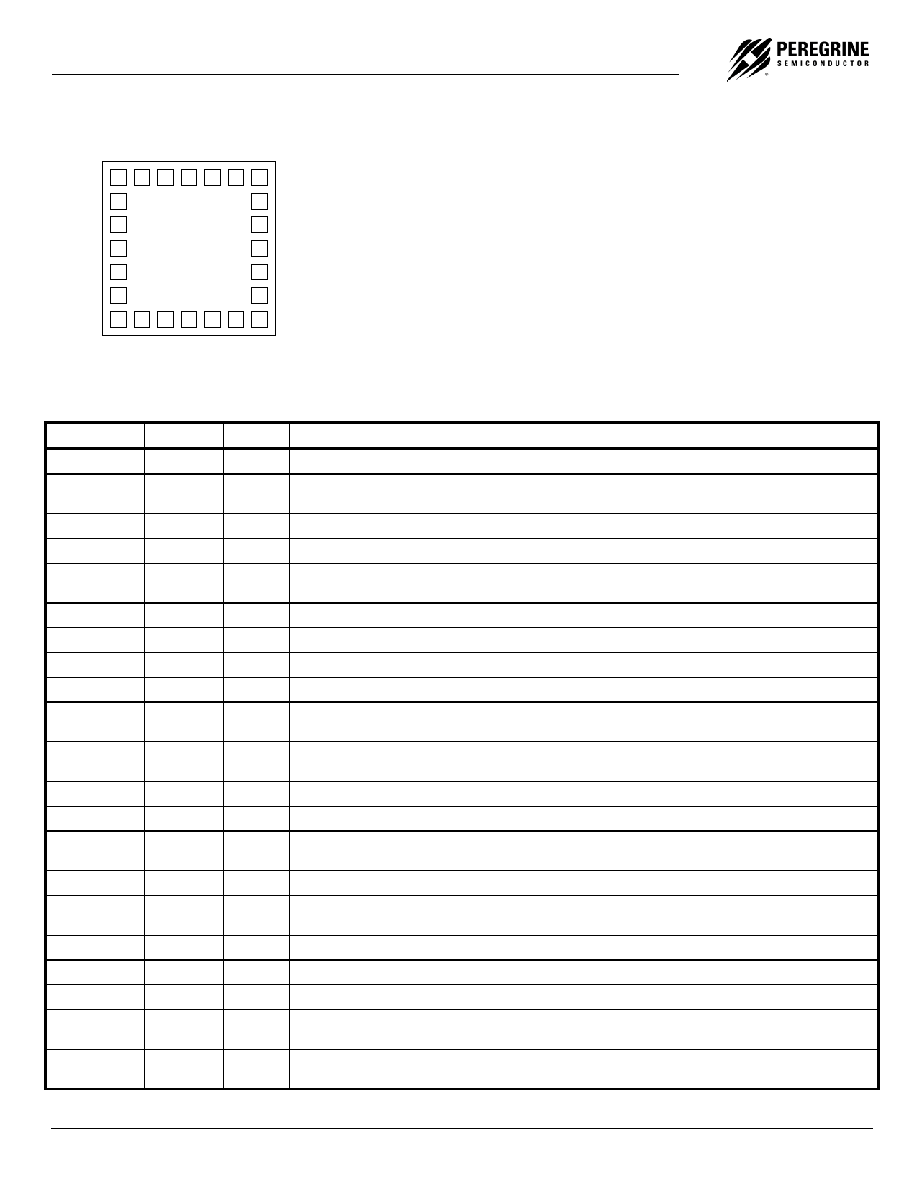
Figure 3. Pin Configuration: 24-Pin BCC (Top View)
Table 2. Pin Descriptions
Pin No.
Pin Name
Type
Description
1
N / C
No connect.
2 CP1
Output
Internal charge-pump output from PLL1 for connection to a loop filter for driving the input of an external
VCO.
3 GND
Ground
4 f
in
1
Input
Prescaler input from the PLL1 (RF) VCO. Maximum frequency is 1.8 GHz.
5 Dec1
Power supply decoupling pin for PLL1. A capacitor should be placed as close as possible to this pin and be
connected directly to the ground plane.
6 V
DD1
PLL1 prescaler power supply (FlexiPower 1).
7
N / C
No connect.
8 f
r
Input
Reference frequency input.
9 GND
Ground.
10 f
o
LD Output
Multiplexed output of the PLL1 and PLL2 main counters or reference counters, Lock Detect signals, and
data out of the shift register. CMOS output (see Table 11, f
o
LD Programming Truth Table).
11 Clock
Input
CMOS clock input. Serial data for the various counters is clocked in on the rising edge into the 21-bit shift
register.
12
Data
Input
Binary serial data input. CMOS input data entered MSB first. The two LSBs are the control bits.
13
N / C
No connect.
14 LE
Input
Load Enable CMOS input. When LE is high, data word stored in the 21-bit serial shift register is loaded into
one of the four appropriate latches (as assigned by the control bits).
15 V
DD2
PLL2 prescaler power supply. 3.3 kohm resistor to V
DD
.
16 Dec2
Power supply decoupling pin for PLL2. A capacitor should be placed as close as possible to this pin and be
connected directly to the ground plane.
17 f
in
2
Input
Prescaler input from the PLL2 (IF) VCO. Maximum frequency is 550MHz.
18 GND
Ground.
19
N / C
No connect.
20 CP2
Output
Internal charge-pump output for PLL2. For connection to a loop filter for driving the input of an external
VCO.
21 V
DD
(Note
1)
Power supply voltage input. Input may range from 2.7 V to 3.3 V. A bypass capacitor should be placed as
close as possible to this pin and be connected directly to the ground plane.
N/C
1
2
3
4
5
6
7
8
9
10
20
19
18
17
16
15
14
13
12
11
21
22
23
24
CP2
V
DD
V
DD
N/C
V
DD
N/C
N/C
Data
Clock
f
o
LD
GND
f
r
N/C
GND
f
in
2
Dec2
V
DD2
LE
CP1
GND
f
in
1
DEC1
V
DD1

PE3293
Product Specification
Copyright
Peregrine Semiconductor Corp. 2003
File No. 70/0015~02C
|
UTSi CMOS RFIC SOLUTIONS
Page 4 of 18
Pin No.
Pin Name
Type
Description
22 V
DD
(Note 1)
Same as pin 21.
23
N / C
No connect.
24 V
DD
(Note 1)
Same as pin 21.
Note 1: V
DD
pins 21, 22, and 24 are connected by diodes and must be supplied with the same voltage level.
PE3293 Description
The PE3293 is intended for such applications as
the local oscillator for the RF and first IF of dual-
conversion transceivers. The RF PLL (PLL1)
includes a 32/33 prescaler with a 1.8 GHz
maximum frequency of operation, where the IF
PLL (PLL2) incorporates a 16/17 prescaler with a
550 MHz maximum frequency of operation. Using
an advanced fractional-N phase-locked loop
technique, the PE3293 can generate a stable,
very low phase- noise signal. The dual fractional
architecture allows fine resolution in both PLLs,
with no degradation in phase noise performance.
Data is transferred into the PE3293 via a three-
wire interface (Data, Clock, LE). Supply voltage
can range from 2.7 to 3.3 volts for V
DD
. PE3293
features very low power consumption and is
available in a JEDEC MO-153-AC (TSSOP), 20-
pin package and 24-lead BCC package.
Spurious
Response
A critical parameter for synthesizer designs is
spurious output. Spurs occur at the integer
multiples of the step size away from center tone.
An important feature of fractional synthesizers is
their ability to reduce these spurious sidebands.
The PE3293 has a built-in method for reducing
these spurs, with no external components or
tuning required. In addition, this circuitry works
over the full commercial temperature and VCO
tuning range.
PE3293
Product Specification
PEREGRINE SEMICONDUCTOR CORP.
|
http://www.peregrine-semi.com
Copyright
Peregrine Semiconductor Corp. 2003
Page 5 of 18
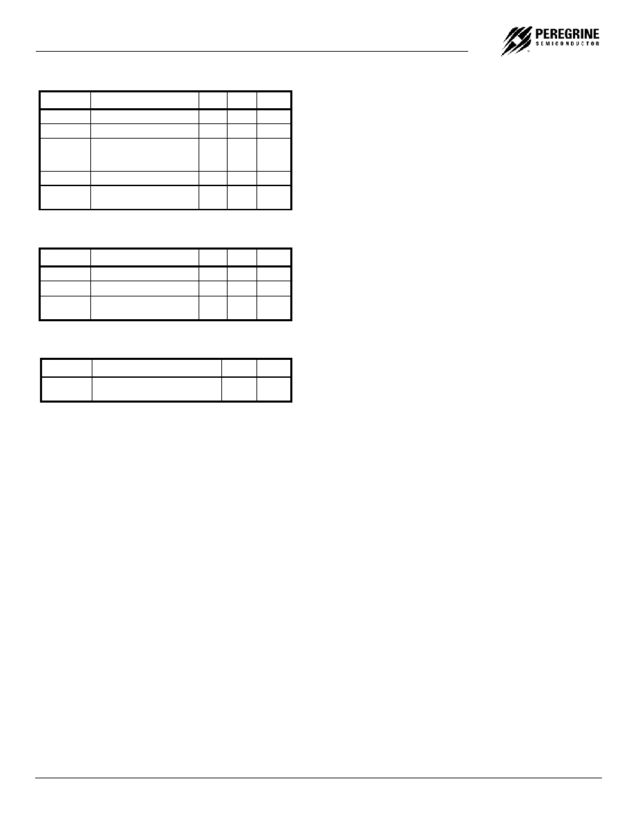
Table 3. Absolute Maximum Ratings
Symbol Parameter/Conditions Min Max Units
V
DD
Supply
voltage
-0.3
4.0 V
V
DDI
, V
DD
2 Prescaler
supply
voltage -0.3 V
DD
V
V
I
Voltage on any input
-0.3
V
DD
+
0.3
V
I
I
DC into any input
-10
+10
mA
T
stg
Storage
temperature
range
-65 150
∞C
Table 4. Operating Ratings
Symbol Parameter/Conditions Min Max Units
V
DD
Supply
voltage
2.7
3.3 V
V
DD
1, V
DD
2 Prescaler
supply
voltage
0.8 V
DD
∞C
T
A
Operating
ambient
temperature range
-40 85
∞C
Table 5. ESD Ratings
Symbol Parameter/Conditions Level
Units
V
ESD
ESD voltage human body
model (Note 1)
2000 V
Note 1: Periodically sampled, not 100% tested. Tested per MIL-
STD-883, M3015 C2
Electrostatic Discharge (ESD) Precautions
When handling this UTSi device, observe the same
precautions that you would use with other ESD-
sensitive devices. Although this device contains
circuitry to protect it from damage due to ESD,
precautions should be taken to avoid exceeding the
rating specified in Table 5.
Latch-Up Avoidance
Unlike conventional CMOS devices, UTSi CMOS
devices are immune to latch-up.