
Page 1 of 8
Document No. 70-0111-03
www.psemi.com
©2005 Peregrine Semiconductor Corp. All rights reserved.
V
DD
= 3.0 V, -40∞ C
T
A
85∞ C,
unless otherwise specified
The PE3501 is a high-performance dynamic UltraCMOSTM
prescaler with a fixed divide ratio of 2. Its operating frequency
range is 400 MHz to 3.5 GHz. The PE3501 operates on a
nominal 3 V supply and draws only 12 mA. It is packaged in a
small 8-lead TSSOP and is ideal for frequency scaling and
microwave PLL synthesis solutions.
The PE3501 is manufactured on Peregrine's UltraCMOSTM
process, a patented variation of silicon-on-insulator (SOI)
technology on a sapphire substrate, offering the performance
of GaAs with the economy and integration of conventional
CMOS.
Product Specification
3500 MHz Low Power UltraCMOSTM
Divide-by-2 Prescaler
Product Description
Figure 1. Functional Schematic Diagram
PE3501
Features
∑
High-frequency operation:
400 MHz to 3500 MHz
∑
Fixed divide ratio of 2
∑
Low-power operation: 12 mA typical
@ 3 V
∑
Small package: 8-lead TSSOP
∑
Low cost
Table 1. Electrical Specifications
(Z
S
= Z
L
= 50
)
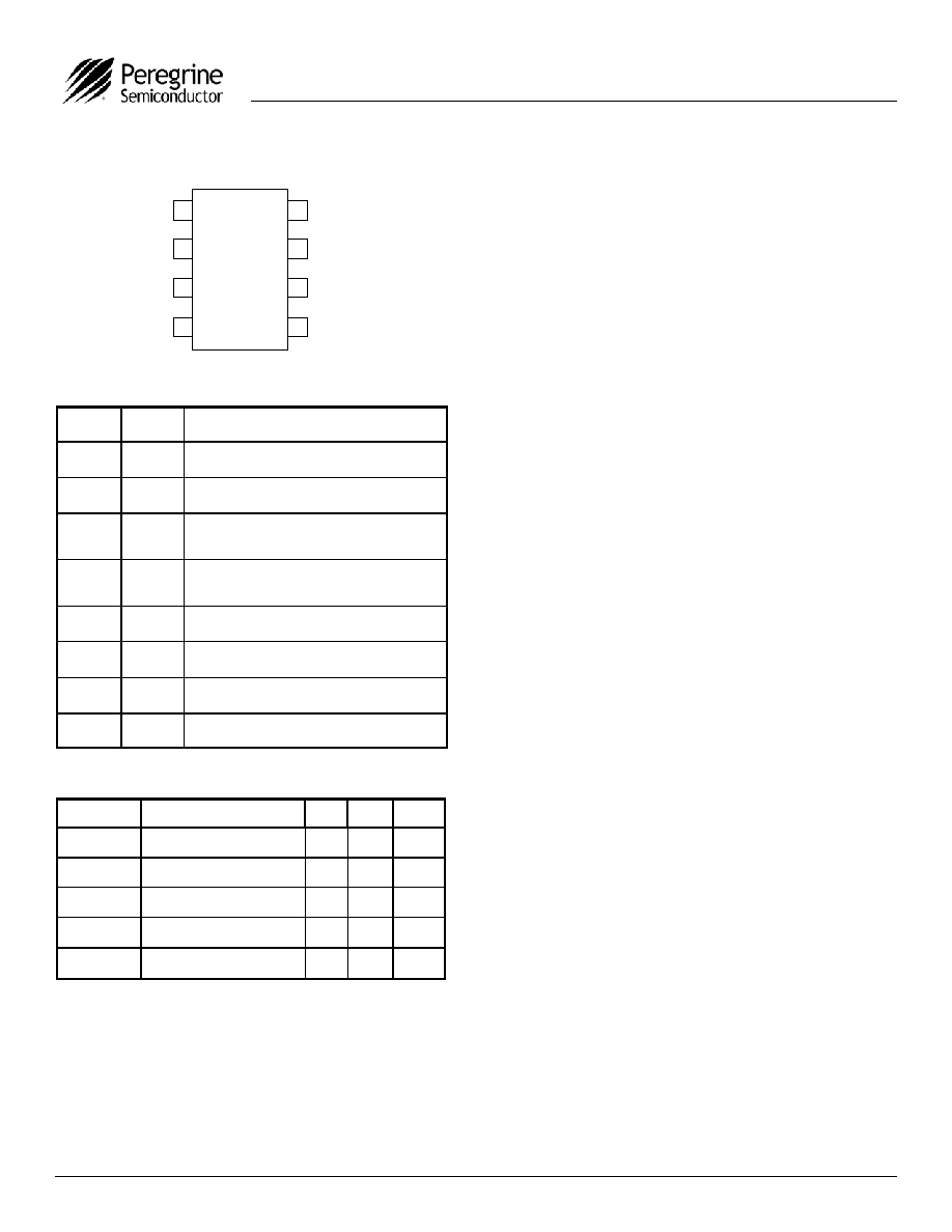
Figure 2. Package Type
8-lead TSSOP
PREAMP
DRIVER
OUTPUT BUFFER
D Q
CLK
DEC QB
OFF-CHIP
BYPASS
F
in
F
out
Parameter Conditions
Minimum
Typical
Maximum
Units
Supply Voltage
2.85
3.0
3.15
V
Supply Current
12
15
mA
Input Frequency (F
in
)
400
3500
MHz
Input Power (P
in
)
400 MHz
F
in
3000 MHz
3000 MHz < F
in
3500 MHz
-10
0
+10
+10
dBm
dBm
Output Power (P
out
)
400 MHz
F
in
3000 MHz
3000 MHz < F
in
3500 MHz
-10
-15
dBm
dBm
Product Specification
PE3501
Page 2 of 8
©2005 Peregrine Semiconductor Corp. All rights reserved.
Document No. 70-0111-03
UltraCMOSTM RFIC Solutions
Table 2. Pin Descriptions
Table 3. Absolute Maximum Ratings
Electrostatic Discharge (ESD) Precautions
When handling this UltraCMOSTM device, observe
the same precautions that you would use with
other ESD-sensitive devices. Although this device
contains circuitry to protect it from damage due to
ESD, precautions should be taken to avoid
exceeding the rating specified in Table 3.
Latch-Up Avoidance
Unlike conventional CMOS devices, UltraCMOSTM
devices are immune to latch-up.
Figure 3. Pin Configuration (Top View)
Device Functional Considerations
The PE3501 divides a 400 MHz to 3500 MHz
input signal by two, producing a 200 MHz to 1750
MHz output signal. To work properly, pin 3 must
be supplied with a bypass capacitor to ground. In
addition, the input and output signals (pins 2 & 7)
must be AC coupled via an external capacitor, as
shown in the test circuit in Figure 4.
The ground pattern on the board should be made
as wide as possible to minimize ground
impedance. See Figure 11 for a layout example.
Absolute Maximum Ratings are those values
listed in the above table. Exceeding these values
may cause permanent device damage. Exposure
to absolute maximum ratings for extended periods
may affect device reliability.
3501
1
2
3
4
8
7
6
5
F
IN
GND
DEC
GND
F
OUT
V
DD
NC
GND
Pin
No.
Pin
Name
Description
1 V
DD
Power supply pin. Bypassing is required.
2 F
in
Input signal pin. DC blocking capacitor
required (15 pF typical)
3 DEC
Power supply decoupling pin. Place a ca-
pacitor as close as possible and connect
directly to the ground plane.
4 GND
Ground pin. Ground pattern on the board
should be as wide as possible to reduce
ground impedance.
5 GND
Ground
pin.
6 NC
No Connection. This pin should be left
open.
7 F
out
Divided frequency output pin. DC blocking
capacitor required (47 pF typical)
8 GND
Ground
pin.
Symbol Parameter/Conditions
Min
Max
Units
V
DD
Supply voltage
4.0
V
P
in
Input
Power
15
dBm
T
ST
Storage temperature range
-65
150
∞C
T
OP
Operating temperature
range
-40 85 ∞C
V
ESD
ESD voltage (Human Body
Model)
250
V
Product Specification
PE3501
Page 3 of 8
©2005 Peregrine Semiconductor Corp. All rights reserved.
Document No. 70-0111-03
www.psemi.com
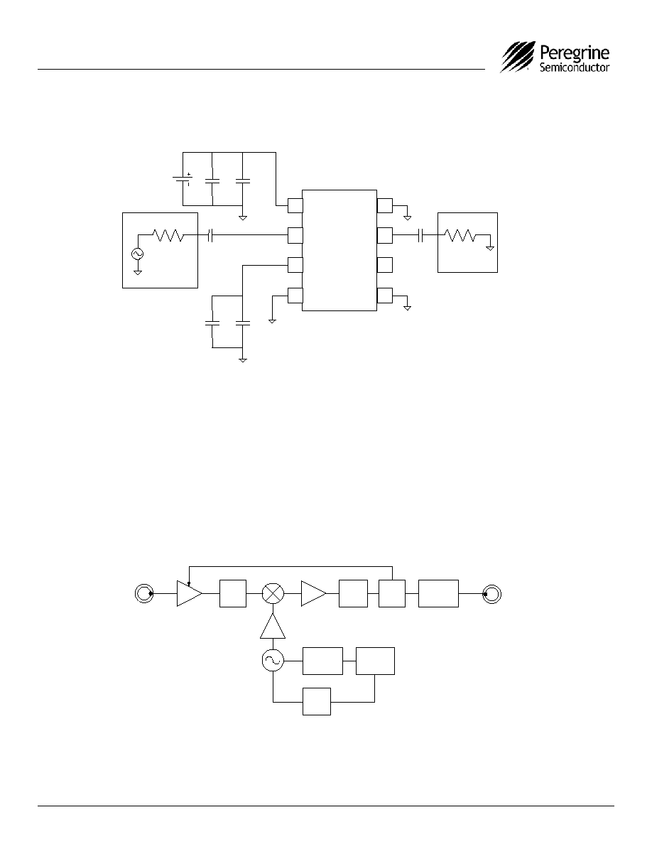
Figure 4. Test Circuit Block Diagram
Figure 5. High Frequency System Application
The wideband frequency of operation of the PE3501 makes it an ideal part for use in a
DBS down-converter system.
Signal Generator
Spectrum
Analyzer
PE3501
1
2
3
4
8
7
6
5
10 pF
15 pF
50
VDD
3 V +/
-
0.15 V
1000 pF
47 pF
10 pF
10 nF
50
N/C
BPF
SA
W
AGC
FM
DEMOD
PE3501
PE3236
LOW NOISE
PLL SYNTH
LPF
INPUT FROM
DBS 1
ST
IF
BASEBAND
OUTPUT
DIVIDE-BY-2

Product Specification
PE3501
Page 5 of 8
©2005 Peregrine Semiconductor Corp. All rights reserved.
Document No. 70-0111-03
www.psemi.com
Table 4. S11
Table 5. S22
Input Freq (GHz) S11 Magnitude (dB)
S11 Angle (deg)
0.4 -0.5523 -9.337
0.5 -0.6707
-11.253
0.6 -0.806
-13.193
0.7 -0.9642 -14.8
0.8 -1.109
-15.929
0.9 -1.1263
-17.103
1.0 -1.152
-18.594
1.1 -1.1703
-20.722
1.2 -1.2353
-22.915
1.3 -1.4078 -25.66
1.4 -1.6207
-28.199
1.5 -1.8965
-30.249
1.6 -2.1032
-31.079
1.7 -1.9731
-32.514
1.8 -1.8229
-36.258
1.9 -1.8517
-40.604
2.0 -2.0308
-44.918
2.1 -2.1353 -48.91
2.2 -2.2884
-53.156
2.3 -2.397
-56.979
2.4 -2.4811
-61.184
2.5 -2.5498
-64.955
2.6 -2.6367
-68.656
2.7 -2.655
-72.265
2.8 -2.7216
-75.379
2.9 -2.691
-78.326
3.0 -2.6813
-80.734
3.1 -2.6933 -82.87
3.2 -2.6638
-84.784
3.3 -2.6461
-86.468
3.4 -2.6266
-87.788
3.5 -2.5917
-89.118
Output Freq
(GHz)
S22 Magnitude (dB) S22 Angle (deg)
0.20 -8.7615
26.726
0.25 -8.2705
21.393
0.30 -7.7885
16.647
0.35 -7.6058
10.297
0.40 -7.7922
6.2004
0.45 -8.2309
2.4335
0.50 -8.5583
-0.3158
0.55 -8.8751
-0.2458
0.60 -8.8599
-3.0515
0.65 -9.1496
-2.6752
0.70 -8.8648
-6.0631
0.75 -9.0828
-5.7925
0.80 -9.2022
-6.8019
0.85 -9.2727
-9.3617
0.90 -9.6494
-12.806
0.95 -9.4383
-14.454
1.00 -9.5217
-16.286
1.05 -9.6043
-19.118
1.10 -9.7282
-23.597
1.15 -9.8069
-25.461
1.20 -9.8221
-29.038
1.25 -9.8694
-32.629
1.30 -9.8693
-34.669
1.35 -9.8667
-40.785
1.40 -9.8509
-43.139
1.45 -9.9141
-46.745
1.50 -9.7063
-51.695
1.55 -9.8686
-54.805
1.60 -9.4836
-56.589
1.65 -9.4498
-62.744
1.70 -9.3233
-66.237
1.75 -9.2206
-66.07
Figure 8. S11 vs. Input Frequency (V
DD
= 3 V)
Figure 9. S22 vs. Output Frequency (V
DD
= 3 V)
Freq (400.0MHz to 3.500GHz)
S(1
,
1
)
Freq (200.0MHz to 1.750GHz)
S
(
2,
2)
