PEREGRINE SEMICONDUCTOR CORP.
|
http://www.peregrine-semi.com
Copyright
Peregrine Semiconductor Corp. 2003
Page 1 of 8
Product Description
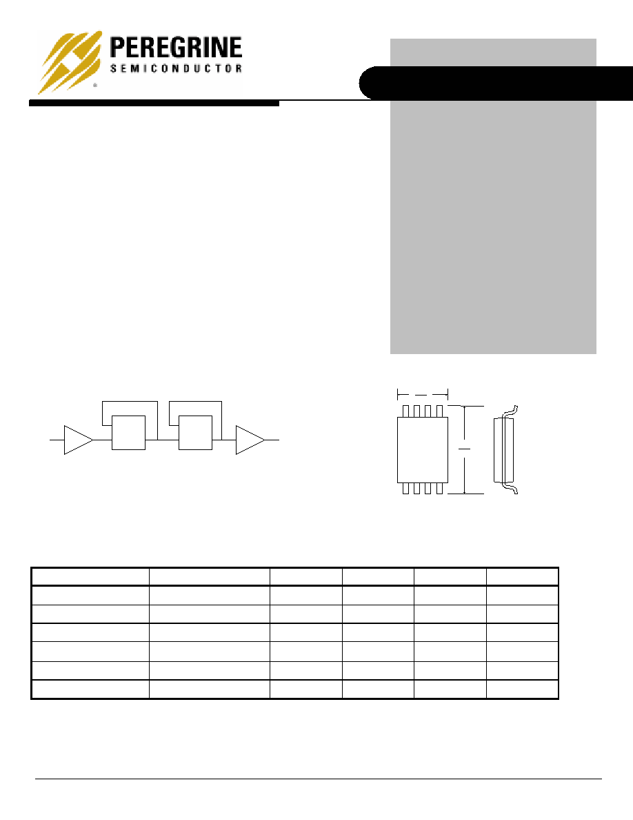
Figure 1. Functional Schematic Diagram
D
QB
Q
CLK
D
QB
Q
CLK
Pre-Amp
Output
Buffer
IN
OUT
Figure 2. Package Drawing
Table 1. Electrical Specifications
(Z
S
= Z
L
= 50
)
V
DD
= 3.0 V, -40
� C < T
A
< 85
� C,
unless otherwise specified
Parameter
Minimum
Typical Maximum Units
Supply Voltage
2.85 3.0 3.15 V
Supply Current
12
17
mA
Input Frequency (F
IN
)
1.5 3.5
GHz
Input Power (P
IN
) 1500
MHz
F
in
3200 MHz
-10
+5
dBm
3200 MHz < F
in
3500 MHz
0
+5
dBm
Output Power
-5
dBm
PRELIMINARY SPECIFICATION
PE3502
3.5 GHz Low Power CMOS
Divide-by-4 Prescaler
Features
� High-frequency operation:
1.5 GHz to 3.5 GHz
� Fixed divide ratio of 4
� Low-power operation: 12 mA
typical @ 3 V across frequency
� Small package: 8-lead MSOP
� Low Cost
The PE3502 is a high performance monolithic CMOS
prescaler with a fixed divide ratio of 4. Its operating
frequency range is 1.5 GHz to 3.5 GHz. The PE3502
operates on a nominal 3 V supply and draws only 12 mA.
It is packaged in a small 8-lead MSOP and is ideal for
microwave PLL synthesis solutions.
The PE3502 is manufactured in Peregrine's patented
Ultra Thin Silicon (UTSi
) CMOS process, offering the
performance of GaAs with the economy and integration
of conventional CMOS.
8-lead MSOP
5.05
4.75
3.05
2.85
PE3502
Preliminary Specification
Copyright
Peregrine Semiconductor Corp. 2003
File No. 70/0046~03A
|
UTSi CMOS RFIC SOLUTIONS
Page 2 of 8
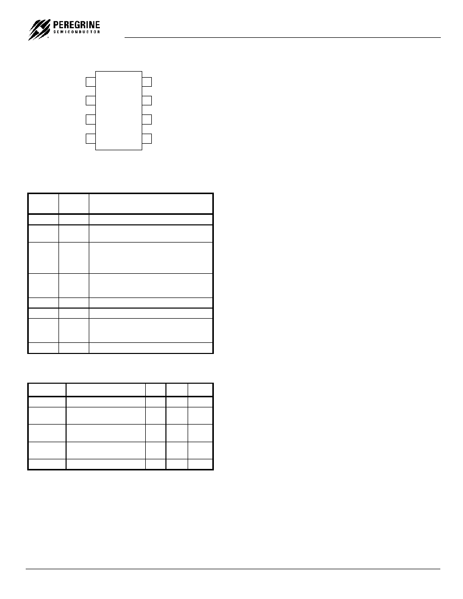
Figure 3. Pin Configuration
Table 2. Pin Descriptions
Pin
No.
Pin
Name
Description
1
VDD
Power supply pin. Bypassing is required.
2
IN
Input signal pin. Should be coupled with a
capacitor (eg 15 pF)
3
DEC
Power supply decoupling pin. Place a
capacitor as close as possible and connect
directly to the ground plane (eg 10 nF and
10 pF).
4
GND
Ground pin. Ground pattern on the board
should be as wide as possible to reduce
ground impedance.
5 GND
Ground
pin.
6 GND
Ground
pin.
7
OUT
Divided frequency output pin. This pin
should be coupled with a capacitor (eg 100
pF).
8 GND
Ground
pin.
Table 3. Absolute Maximum Ratings
Symbol Parameter/Conditions Min Max Units
VDD Supply
voltage
4.0 V
T
ST
Storage
temperature
range
-65 150
�C
T
OP
Operating
temperature
range
-40 85
�C
VESD
ESD voltage (Human
Body Model)
250
V
P
INMAX
Maximum input power
10
dBm
Electrostatic Discharge (ESD) Precautions
When handling this UTSi device, observe the same
precautions that you would use with other ESD-
sensitive devices. Although this device contains
circuitry to protect it from damage due to ESD,
precautions should be taken to avoid exceeding the
rating specified in Table 3.
Latch-Up Avoidance
Unlike conventional CMOS devices, UTSi CMOS
devices are immune to latch-up.
Device Functional Considerations
The PE3502 takes an input signal frequency from
1.5 GHz to 3.5 GHz and produces an output signal
frequency one-fourth that of the supplied input. In
order for the prescaler to work properly, several
conditions need to be adhered to. It is crucial that
pin 3 be supplied with a bypass capacitor to
ground. In addition, the input and output signals
(pins 2 & 7, respectively) need to be AC coupled
via an external capacitor as shown in the test
circuit in Figure 7.
The ground pattern on the board should be made
as wide as possible to minimize ground
impedance.
PE3502
1
2
3
4
8
7
6
5
IN
GND
DEC
GND
OUT
VDD
GND
GND

PE3502
Preliminary Specification
PEREGRINE SEMICONDUCTOR CORP.
|
http://www.peregrine-semi.com
Copyright
Peregrine Semiconductor Corp. 2003
Page 3 of 8
8
9
10
11
12
13
14
15
0.5
1.5
2.5
3.5
4.5
Frequency (GHz)
Cur
r
e
nt (mA)
Typical Performance Data
Figure 4. Input Sensitivity
Figure 5. Device Current
Figure 6. Output Power
-30
-25
-20
-15
-10
-5
0
0.5
1.5
2.5
3.5
4.5
Frequency (GHz)
-3.0
-2.0
-1.0
0.0
1.0
2.0
3.0
0.5
1.5
2.5
3.5
4.5
Frequency (GHz)
Powe
r (dBm)
-40C
25C
85C
85C
25C
-40C
-40C
25C
85C
PE3502
Preliminary Specification
Copyright
Peregrine Semiconductor Corp. 2003
File No. 70/0046~03A
|
UTSi CMOS RFIC SOLUTIONS
Page 4 of 8
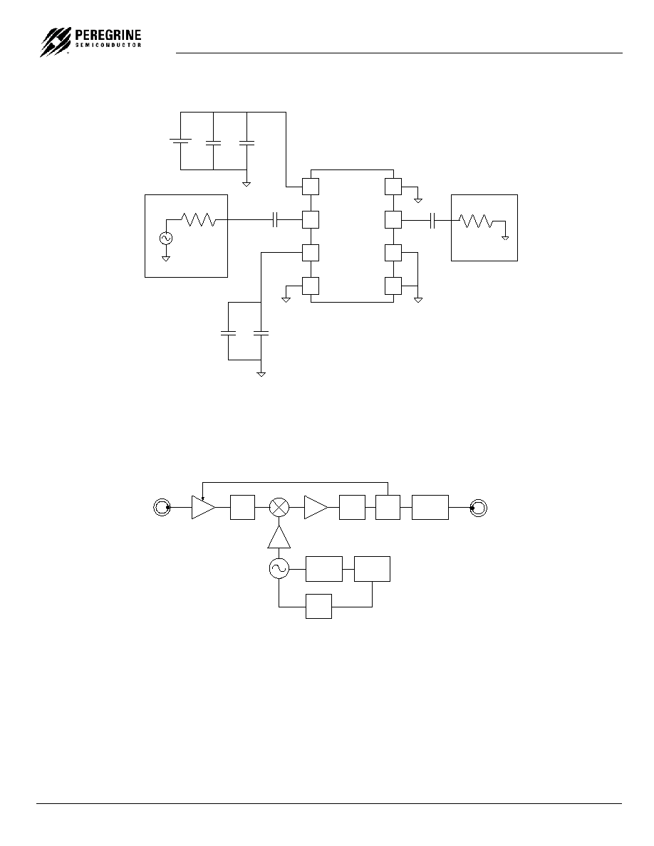
Figure 7. Test Circuit Block Diagram
Figure 8. High Frequency System Application
The wideband frequency of operation of the PE3502 makes it an ideal part for use in a DBS downconverter
system.
BPF
SAW
AGC
FM
DEMOD
PE3502
PE3293
LOW NOISE
PLL SYNTH
LPF
INPUT FROM
DBS 1
ST
IF
BASEBAND
OUTPUT
DIVIDE-BY-4
Signal Generator
Spectrum
Analyzer
PE3502
1
2
3
4
8
7
6
5
10 pF
15 pF
50
VDD
3 V +/- 0.15 V
1000 pF
100 pF
10 pF
10 nF
50
+
-
PE3502
Preliminary Specification
PEREGRINE SEMICONDUCTOR CORP.
|
http://www.peregrine-semi.com
Copyright
Peregrine Semiconductor Corp. 2003
Page 5 of 8
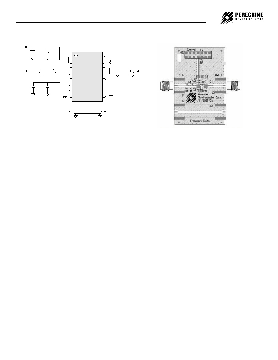
VDD
IN
DEC
GND
GND
OUT
NC
GND
1000 pF
J2-7
J3
J4
J5
10 pF
C1
J1
10 pF
10 nF
C2
Figure 9. Evaluation Board Schematic Diagram
Figure 10. Evaluation Board Layout
Evaluation Kit Operation
The MSOP Prescaler Evaluation Board was
designed to help customers evaluate the PE3502
Divide-by-4 Prescaler. On this board, the device
input (pin 2) is connected to connector J1 through
a 50 transmission line. A series capacitor (C3)
provides the necessary DC block for the device
input. It is important to note that the value of this
capacitance will impact the performance of the
device. A value of 15pF was found to be optimal
for this board layout; other applications may
require a different value.
The device output (pin 7) is connected to
connector J3 through a 50 transmission line. A
series capacitor (C1) provides the necessary DC
block for the device output. Note that this
capacitor must be chosen to have a low
impedance at the desired output frequency the
device. The value of 100pF was chosen to
provide a wide operating range for the evaluation
board.
The board is constructed of a two-layer FR4
material with a total thickness of 0.031". The
bottom layer provides ground for the RF
transmission lines. The transmission lines were
designed using a coplanar waveguide above
ground plane model with trace width of 0.030",
trace gaps of 0.007", dielectric thickness of 0.028",
metal thickness of 0.0014" and
r
of 4.4. Note that
the predominate mode for these transmission lines
is coplanar waveguide.
J2 provides DC power to the device. Starting from
the lower left pin, the second pin to the right (J2-3)
is connected to the device VDD pin (1). Two
decoupling capacitors (10 pF, 1000 pF) are
included on this trace. It is the responsibility of the
customer to determine proper supply decoupling
for their design application.
The DEC pin (3) must be connected to a low
impedance AC ground for proper device operation.
On the board, two decoupling capacitors (C6 = 10
nF, C4 = 10 pF), located on the back of the board,
perform this function.
Applications Support
If you have a problem with your evaluation kit or if
you have applications questions call (858) 455-
0660 and ask for applications support. You may
also contact us by fax or e-mail:
Fax: (858) 455-0770
E-Mail: help@peregrine-semi.com
C3
C1