 | –≠–ª–µ–∫—Ç—Ä–æ–Ω–Ω—ã–π –∫–æ–º–ø–æ–Ω–µ–Ω—Ç: PE4122-00 | –°–∫–∞—á–∞—Ç—å:  PDF PDF  ZIP ZIP |

PEREGRINE SEMICONDUCTOR CORP.
|
http://www.peregrine-semi.com
Copyright
Peregrine Semiconductor Corp. 2003
Page 1 of 8
Product Description
Figure 1. Functional Schematic Diagram
PE4122
RF
LO
IF
Figure 2. Package Type
Table 1. Electrical Specifications @ +25 ∞C
(Z
S
= Z
L
= 50
)
Parameter Minimum
Typical Maximum Units
Frequency Range:
LO
RF
IF*
1540
1800
--
--
--
260
1740
2000
--
MHz
MHz
MHz
Conversion Loss**
7.4
7.8
dB
Isolation:
LO-RF
LO-IF
28
34
34
38
dB
dB
Input IP3
1.8 GHz
1.9 GHz
2.0 GHZ
28
31
28
30
33
30
dBm
dBm
dBm
Input 1 dB Compression
20
dBm
*An IF frequency of 260MHz is a nominal frequency. The IF frequency can be specified by the user as long as the RF and LO frequencies are within the specified maximum
and minimum.
**Conversion Loss includes loss of IF transformer (M/A COM ETK4-2T, nominal loss 0.7dB at 260MHz).
Test conditions unless otherwise noted: LO = 260MHz, LO input drive = 17dBm, RF input drive = 0dBm.
PRODUCT SPECIFICATION
PE4122
High Linearity Quad MOSFET
Mixer For PCS & 3G BTS
Features
∑ Integrated, single-ended RF &
LO interfaces
∑ High linearity: IIP3 >+ 30 dBm,
1.8
- 2.0 GHz (+17 dBm LO)
∑ Low-conversion loss: 7.4 dB
(+17 dBm LO)
∑ High isolation: typical LO-IF at
38 dB, LO-RF at 34 dB
∑ Designed for low-side LO
injection
The PE4122 is a high linearity, passive Quad MOSFET
Mixer for PCS & 3G Base Station Receivers, exhibiting
high dynamic range performance over a broad LO drive
range up to +20 dBm. This mixer integrates passive
matching networks to provide single-ended interfaces for
the RF and LO ports, eliminating the need for external
RF baluns or matching networks. The PE4122 is
optimized for frequency down-conversion using low-side
LO injection for PCS & 3G Base Station applications, and
is also suitable for use in up-conversion applications.
The PE4122 is manufactured in Peregrine's patented
Ultra-Thin Silicon (UTSi
) CMOS process, offering the
performance of GaAs with the economy and integration
of conventional CMOS.
8-lead
TSSOP
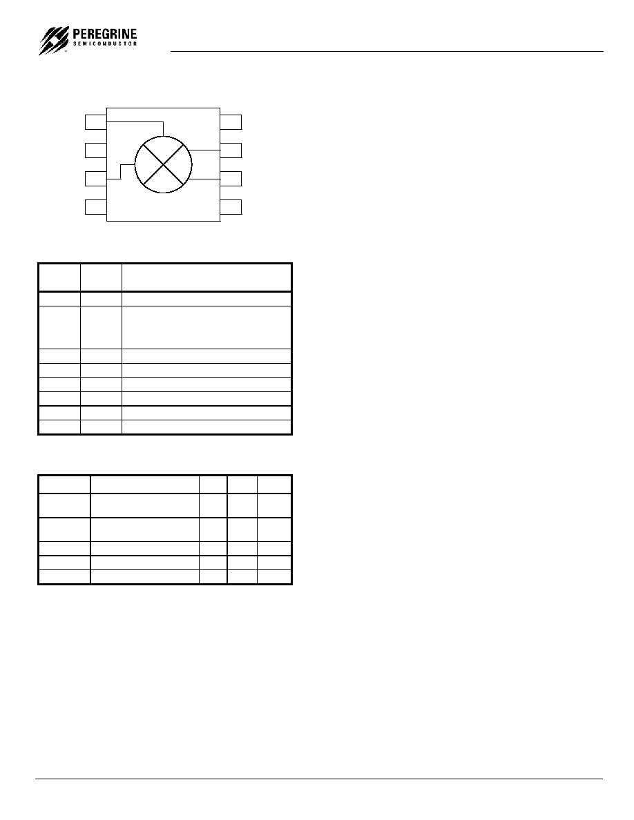
PE4122
Product Specification
Copyright
Peregrine Semiconductor Corp. 2003
File No. 70/0041~03A
|
UTSi CMOS RFIC SOLUTIONS
Page 2 of 8
Figure 3. Pin Configuration
PE4122
5
6
7
8
4
3
2
1
GND
RF
GND
LO
GND
IF2
IF1
GND
Table 2. Pin Descriptions
Pin
No.
Pin
Name
Description
1 LO
LO
Input
2
GND
Ground connection for Mixer. Traces
should be physically short and connect
immediately to ground plane for best
performance.
3 RF
RF
Input
4 GND
Ground.
5 GND
Ground.
6
IF2
IF differential output
7
IF1
IF differential output
8 GND
Ground.
Table 3. Absolute Maximum Ratings
Symbol Parameter/Conditions Min Max Units
T
ST
Storage temperature
range
-65 150
∞C
T
OP
Operating temperature
range
-40 85
∞C
P
LO
LO input power
20
dBm
P
RF
RF input power
16
dBm
V
ESD
ESD Sensitive Device
250
V
Electrostatic Discharge (ESD) Precautions
When handling this UTSi device, observe the same
precautions that you would use with other ESD-
sensitive devices. Although this device contains
circuitry to protect it from damage due to ESD,
precautions should be taken to avoid exceeding the
rating specified in Table 3.
Latch-Up Avoidance
Unlike conventional CMOS devices, UTSi CMOS
devices are immune to latch-up.
PE4122
Product Specification
PEREGRINE SEMICONDUCTOR CORP.
|
http://www.peregrine-semi.com
Copyright
Peregrine Semiconductor Corp. 2003
Page 3 of 8
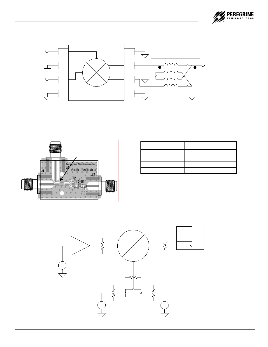
IF
PE4122
GND
IF2
IF1
GND
GND
RF
GND
LO
LO
IF
RF
4122
Eval
Board
Sig
Gen
Sig
Gen
Hybrid
Tee
3 dB
PA
Sig
Gen
3 dB
Spectrum
Analyzer
3 dB
6 dB
6 dB
Figure 4. Evaluation Board Schematic Diagram
T2 M/A-Com E-Series RF 4:1 Transformer 2.0 ≠ 1000 MHz ETK4-2T
Figure 5. Evaluation Board Layout
Table 4. Bill of Materials
Reference
Value / Description
T2
M/A Com ETK4-2T
U1 (Not Labeled)
PE4122 Mixer
R1 0
J1, J2, J3
SMA Connector
Figure 6. Evaluation Board Testing Block Diagram, 2-Tone Setup
Pin 1
T2

PE4122
Product Specification
Copyright
Peregrine Semiconductor Corp. 2003
File No. 70/0041~03A
|
UTSi CMOS RFIC SOLUTIONS
Page 4 of 8
0
5
10
15
20
25
30
35
40
1800
1850
1900
1950
2000
II
P
3
(
d
B
m
)
Frequency (MHz)
-40!C
85!C
25!C
0
5
10
15
20
25
30
1800
1850
1900
1950
2000
OI
P
3
(
d
B
m
)
Frequency (MHz)
-40!C
85!C
25!C
0
5
10
15
20
25
30
1800
1850
1900
1950
2000
1dB Co
m
p
r
e
s
s
i
o
n (
d
B
m
)
Frequency (MHz)
85!C
-40!C
25!C
-10
-8
-6
-4
-2
0
1800
1850
1900
1950
2000
Frequency (MHz)
-40!C
25!C
85!C
Conv
er
s
i
o
n
Los
s
(
d
B
)
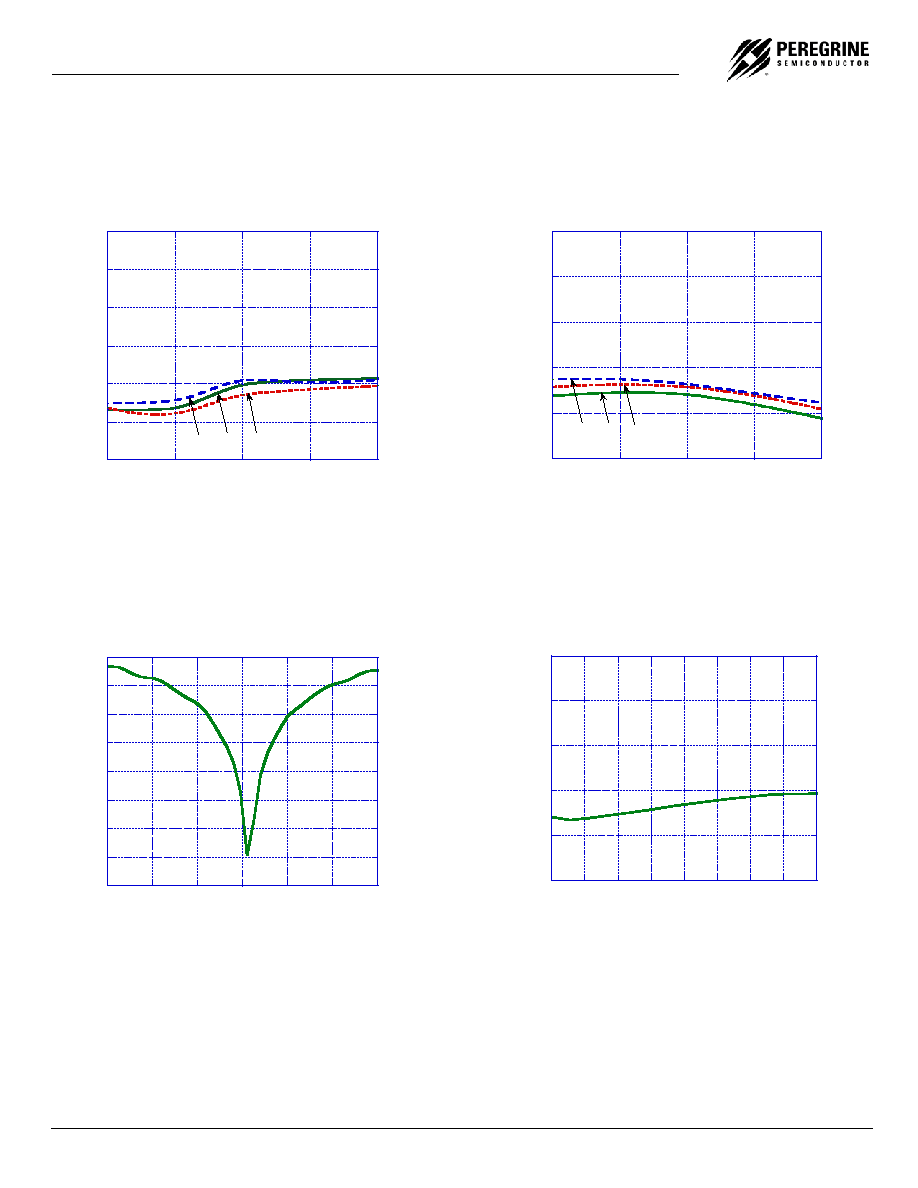
Typical Performance Data (LO=17dBm, RF=0dBm, IF=260MHz)
Figure 7. Conversion Loss vs. Frequency
Figure 8. Input 1dB Compression vs. Frequency
Figure 9. Input IP3 vs. Frequency
Figure 10. Output IP3 vs. Frequency
PE4122
Product Specification
PEREGRINE SEMICONDUCTOR CORP.
|
http://www.peregrine-semi.com
Copyright
Peregrine Semiconductor Corp. 2003
Page 5 of 8
-60
-50
-40
-30
-20
-10
0
1800
1850
1900
1950
2000
LO
-
I
F
Is
ol
a
t
i
on
(
d
B
)
Frequency (MHz)
-40!C
85!C
25!C
-40
-35
-30
-25
-20
-15
-10
-5
0
1.5
1.55
1.6
1.65
1.7
1.75
1.8
R
e
t
u
r
n
L
o
ss
(
d
B
)
Frequency (GHz)
-50
-40
-30
-20
-10
0
1800
1850
1900
1950
2000
LO
-
R
F
I
s
o
l
at
i
o
n
(
d
B
)
Frequency (MHz)
-40!C
85!C
25!C
-25
-20
-15
-10
-5
0
1.7
1.75
1.8
1.85
1.9
1.95
2
2.05
2.1
R
e
t
u
r
n
L
o
ss
(d
B
)
Frequency (GHz)
Typical Performance Data (LO=17dBm, RF=0dBm, IF=260MHz)
Figure 11. LO-IF Isolation vs. Temperature
Figure 12. LO-RF Isolation vs. Temperature
Figure 13. LO Port Return Loss @ 25∞C
Figure 14. RF Port Return Loss @ 25∞C