PEREGRINE SEMICONDUCTOR CORP.
|
http://www.peregrine-semi.com
Copyright
Peregrine Semiconductor Corp. 2003
Page 1 of 7
Product Description
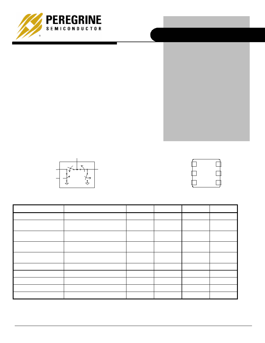
Figure 1. Functional Schematic Diagram
RFCommon
RF1
RF2
CTRL
Figure 2. Package Type
6-lead
MLPM
3x3 mm
4
5
6
3
2
1
Table 1. Electrical Specifications @ +25 ∞C, V
DD
= 3 V
(Z
S
= Z
L
= 50
)
Parameter Conditions
Minimum
Typical
Maximum
Units
Operation Frequency
1
DC
4000 MHz
Insertion Loss
1000 MHz
2000 MHz
0.6
0.7
0.75
0.85
dB
dB
Isolation ≠ RFCommon to
RF1/RF2
1000 MHz
2000 MHz
39
30
42
32
dB
dB
Isolation ≠ RF1 to RF2
1000 MHz
2000 MHz
34
27
36
29
dB
dB
Return Loss
1000 MHz
2000 MHz
21
20
23
22
dB
dB
`ON' Switching Time
CTRL to 0.1 dB final value, 2 GHz
200
ns
`OFF' Switching Time
CTRL to 25 dB isolation, 2 GHz
90
ns
Video Feedthrough
2
15 mV
pp
Input 1 dB Compression
2000 MHz
26
27
dBm
Input IP3
2000 MHz, 14 dBm
43
45
dBm
Notes: 1. Device linearity will begin to degrade below 10 MHz.
2. The DC transient at the output of any port of the switch when the control voltage is switched from Low to High or High to Low in a 50
test set-up, measured with 1ns risetime pulses and 500 MHz bandwidth.
PRODUCT SPECIFICATION
PE4245
SPDT MOSFET RF Switch
Features
∑ Single 3.0 V Power Supply
∑ Low insertion loss: 0.6 dB at
1.0 GHz, 0.7 dB at 2.0 GHz
∑ High isolation of 42 dB at 1.0
GHz, 32 dB at 2.0 GHz
∑ Typical 1 dB compression of
+27 dBm
∑ Single-pin CMOS logic control
∑ Small 3x3mm MLPM package
The PE4245 MOSFET RF Switch is designed to cover a
broad range of applications from DC to 4.0 GHz. This switch
integrates on-board CMOS control logic with a low voltage
CMOS compatible control input. Using a +3-volt nominal
power supply voltage, a 1 dB compression point of +27 dBm
can be achieved. The PE4245 also exhibits excellent
isolation of better than 42 dB at 1.0 GHz and is offered in a
small 3x3 MLPM package.
The PE4245 MOSFET RF Switch is manufactured in
Peregrine's patented Ultra Thin Silicon (UTSi
) CMOS
process, offering the performance of GaAs with the economy
and integration of conventional CMOS.
PE4245
Product Specification
Copyright
Peregrine Semiconductor Corp. 2003
File No. 70/0104~02A
|
UTSi CMOS RFIC SOLUTIONS
Page 2 of 7
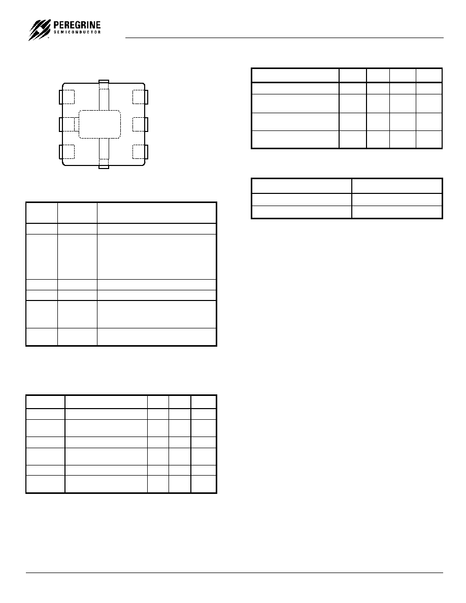
Figure 3. Pin Configuration (top view)
Exposed Solder
Pad - Shorted
to Pin 2
(bottom side)
RF2
GND
RF1
RFCommon
CTRL
V
DD
4
5
6
3
2
1
Table 2. Pin Descriptions
Pin No.
Pin
Name
Description
1
RF2
RF2 port (Note 1)
2
GND
Ground Connection. Traces should be
physically short and connected to the
ground plane. This pin is connected to
the exposed solder pad that also must
be soldered to the ground plane for best
performance.
3
RF1
RF1 port (Note 1)
4 V
DD
Nominal 3 V supply connection.
5
CTRL
CMOS logic level:
High = RFCommon to RF1 signal path
Low = RFCommon to RF2 signal path
6 RF
Common
Common RF port for switch (Note 1)
Note 1: All RF pins must be DC blocked with an external
series capacitor or held at 0 V
DC
.
Table 3. Absolute Maximum Ratings
Symbol Parameter/Conditions Min
Max
Units
V
DD
Power supply voltage
-0.3
4.0
V
V
I
Voltage on any input
-0.3
V
DD
+
0.3
V
T
ST
Storage temperature range
-65
150
∞C
T
OP
Operating
temperature
range
-40 85
∞C
P
IN
Input power (50)
30
dBm
V
ESD
ESD voltage (Human Body
Model)
1500 V
Table 4. DC Electrical Specifications
Parameter Min
Typ
Max
Units
V
DD
Power Supply Voltage
2.7
3.0
3.3
V
I
DD
Power Supply Current
V
DD
= 3V, V
CNTL
= 3V
250
500 nA
Control Voltage High
0.7x
V
DD
V
Control Voltage Low
0.3x
V
DD
V
Table 5. Control Logic Truth Table
Control Voltage
Signal Path
CTRL = CMOS High
RFCommon to RF1
CTRL = CMOS Low
RFCommon to RF2
Electrostatic Discharge (ESD) Precautions
When handling this UTSi device, observe the same
precautions that you would use with other ESD-
sensitive devices. Although this device contains
circuitry to protect it from damage due to ESD,
precautions should be taken to avoid exceeding the
rating specified.
Latch-Up Avoidance
Unlike conventional CMOS devices, UTSi CMOS
devices are immune to latch-up.
PE4245
Product Specification
PEREGRINE SEMICONDUCTOR CORP.
|
http://www.peregrine-semi.com
Copyright
Peregrine Semiconductor Corp. 2003
Page 3 of 7
-1.5
-1.2
-0.9
-0.6
-0.3
0
0
800
1600
2400
3200
4000
I
n
s
e
r
t
i
o
n L
o
s
s
(
d
B
)
Frequency (MHz)
-40∞C
25∞C
85∞C
20
30
40
50
60
20
30
40
50
60
0
800
1600
2400
3200
4000
II
P3
(
d
B
m
)
1d
B
C
o
m
p
r
e
s
s
io
n
Po
i
n
t
(
d
Bm
)
Frequency (MHz)
-100
-80
-60
-40
-20
0
0
800
1600
2400
3200
4000
Is
o
l
a
t
io
n
(
d
B)
Frequency (MHz)
-1.5
-1.2
-0.9
-0.6
-0.3
0
0
800
1600
2400
3200
4000
I
n
s
e
rt
i
o
n
L
o
s
s
(d
B)
Frequency (MHz)
-40∞C
25∞C
85∞C
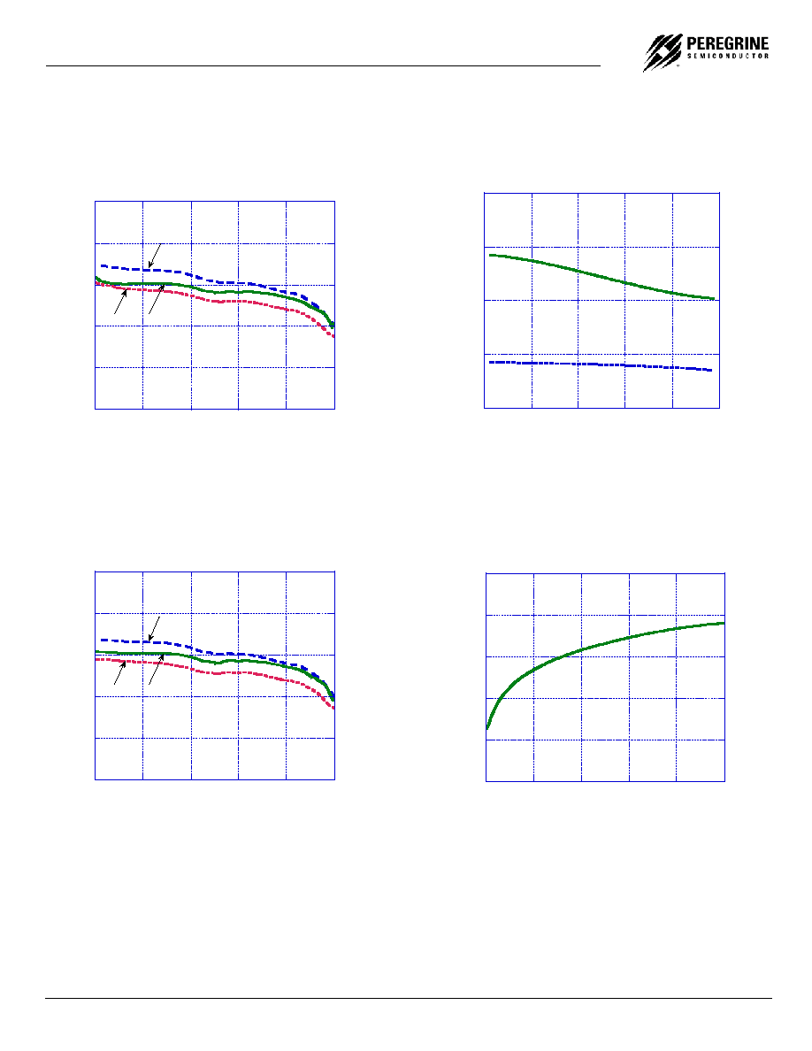
Typical Performance Data @ -40
∞C to 85 ∞C (Unless Otherwise Noted)
Figure 4. Insertion Loss ≠ RFC to RF1
Figure 5. Input 1 dB Compression Point & IIP3
Figure 6. Insertion Loss ≠ RFC to RF2
Figure 7. Isolation ≠ RFC to RF1
PE4245
Product Specification
Copyright
Peregrine Semiconductor Corp. 2003
File No. 70/0104~02A
|
UTSi CMOS RFIC SOLUTIONS
Page 4 of 7
-40
-30
-20
-10
0
0
800
1600
2400
3200
4000
R
e
t
u
rn
L
o
ss
(d
B
)
Frequency (MHz)
RF2
RF1
-40
-30
-20
-10
0
0
800
1600
2400
3200
4000
R
e
t
u
rn
L
o
ss
(d
B
)
Frequency (MHz)
RF2
RF1
-100
-80
-60
-40
-20
0
0
800
1600
2400
3200
4000
Is
o
l
a
t
io
n
(
d
B)
Frequency (MHz)
-100
-75
-50
-25
0
0
800
1600
2400
3200
4000
Is
ol
a
t
i
o
n
(
d
B
)
Frequency (MHz)
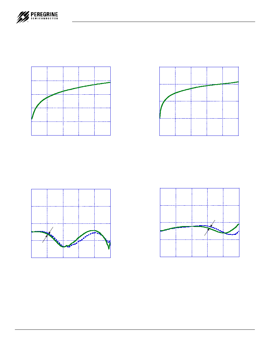
Typical Performance Data @ -40
∞C to 85 ∞C (Unless Otherwise Noted)
Figure 8. Isolation ≠ RFC to RF2
Figure 9. Isolation ≠ RF1 to RF2, RF2 to RF1
Figure 10. Return Loss ≠ RFC to RF1, RF2
Figure 11. Return Loss ≠ RF1, RF2
PE4245
Product Specification
PEREGRINE SEMICONDUCTOR CORP.
|
http://www.peregrine-semi.com
Copyright
Peregrine Semiconductor Corp. 2003
Page 5 of 7
VDD
CNTL
RF1
RFC
GND
RF2
J6-7
J2
J1
J3
J4
J5
J6-3
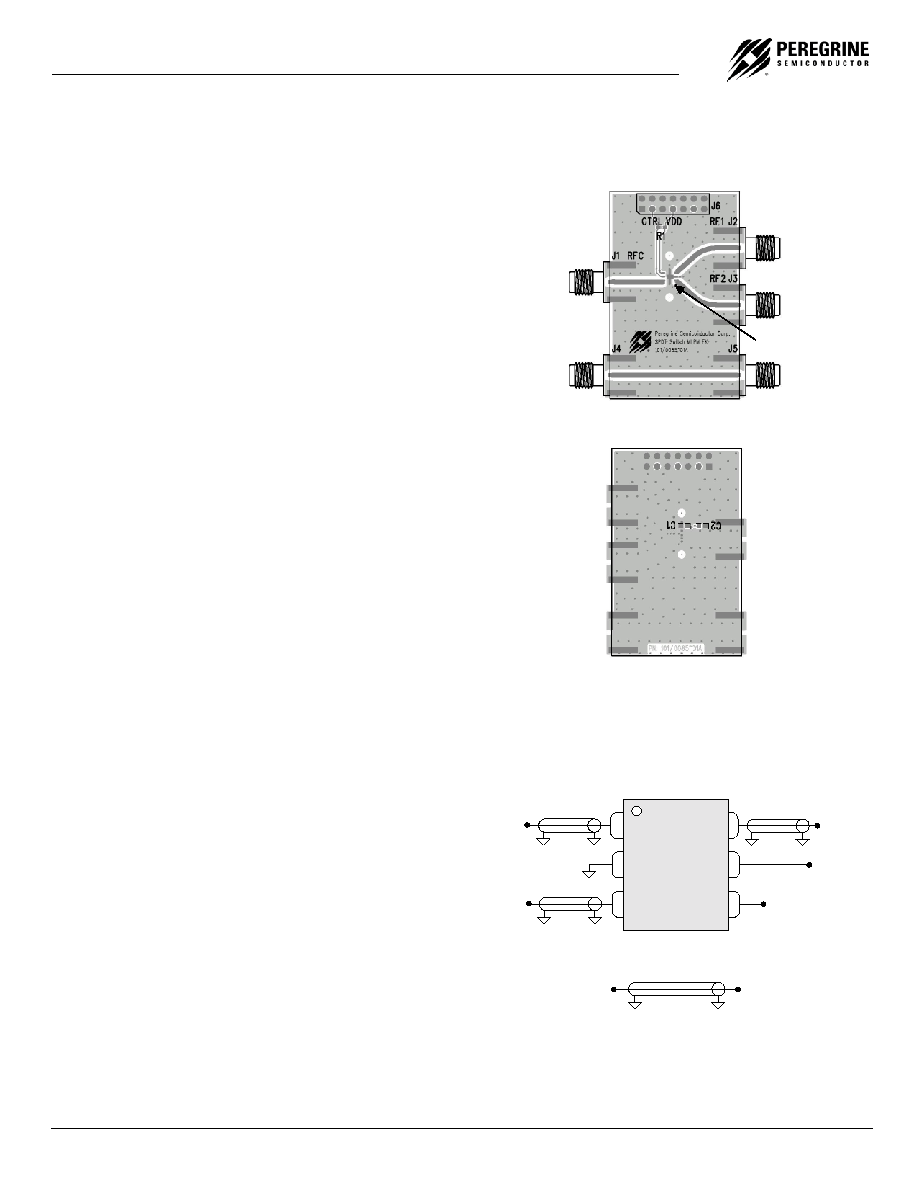
Evaluation Kit Information
Evaluation Kit
The SPDT Switch Evaluation Kit board was
designed to ease customer evaluation of the
PE4245 SPDT switch. The RF common port is
connected through a 50 transmission line to the
top left SMA connector, J1. Port 1 and Port 2 are
connected through 50 transmission lines to the
top two SMA connectors on the right side of the
board, J2 and J3. A through transmission line
connects SMA connectors J4 and J5. This
transmission line can be used to estimate the loss
of the PCB over the environmental conditions
being evaluated.
The board is constructed of a two metal layer FR4
material with a total thickness of 0.031". The
bottom layer provides ground for the RF
transmission lines. The transmission lines were
designed using a coplanar waveguide with ground
plane model using a trace width of 0.0476", trace
gaps of 0.030", dielectric thickness of 0.028",
metal thickness of 0.0021" and
r
of 4.4.
J6 provides a means for controlling DC and digital
inputs to the device. Starting from the lower left
pin, the second pin to the right (J6-3) is connected
to the device CNTL input. The fourth pin to the
right (J6-7) is connected to the device V
DD
input.
Figure 12. Evaluation Board Layouts
Figure 13. Evaluation Board Schematic
Pin 1
PE4245
Product Specification
Copyright
Peregrine Semiconductor Corp. 2003
File No. 70/0104~02A
|
UTSi CMOS RFIC SOLUTIONS
Page 6 of 7
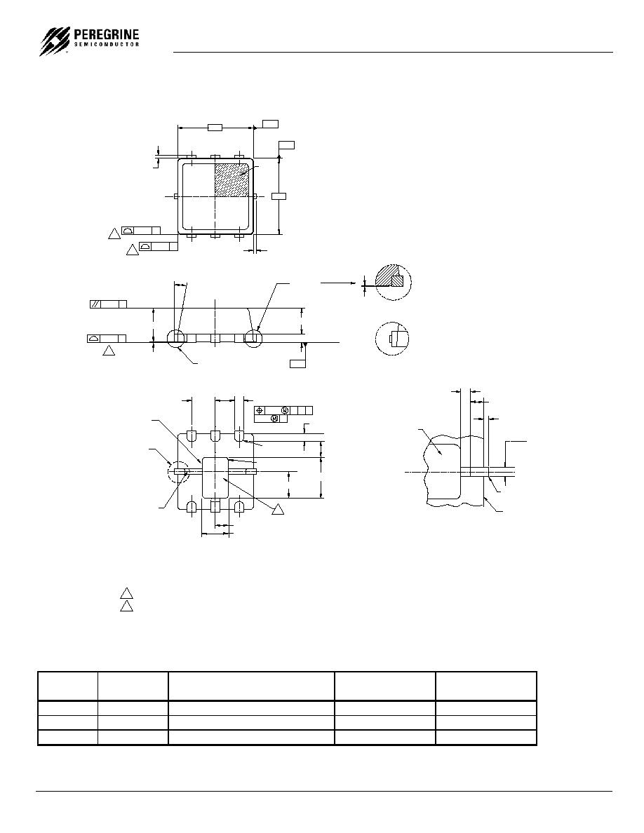
EDGE OF PLASTIC BODY
THIS FEATURE
APPLIES TO
BOTH ENDS OF
THE PKG.
DETAIL A
EXPOSED SLUG/
HEAT SINK
EXPOSED METALIZED
FEATURE
0.17 MIN.
0.29 +0.16
-0.09
0.125 MAX.
0.17
0.30
0.025
±0.025
DETAIL B
(2X)
EXPOSED
3
2
3
BOTTOM VIEW
5
4
1
6
0.10
C A B
0.05
C
0.95
L
C
0.35 +0.08
-0.02
0.29 +0.16
-0.09
1.54 ±0.10
0.96 ±0.10
0.46 ±0.10
0.92 ±0.10
EXPOSED PAD
SEE DETAIL A
R 0.127 TYP
R 0.15 TYP
SEATING
PLANE
SIDE VIEW
TOP VIEW
- C -
0.100 C
0.080 C
0.70 ± 0.05
0.20 ±0.05
0.90 ±0.10
0.025±0.025
10∞+2∞
-10∞
DETAIL C
SEE DETAIL B
3
4
PIN 1
MARK
CL
CL
3.00
0.125
3.00
0.125
0.10 C
0.10 C
5
6
3
2
1
4
4
- A -
- B -
3 COPLANARITY APPLIES TO EXPOSED HEAT SLUG AS WELL AS THE TERMINALS.
4 PROFILE TOLERANCE APPLIES TO PLASTIC BODY ONLY.
1. DIMENSIONS AND TOLERANCES ARE PER ANSi Y14.5
2. DIMENSIONS ARE IN MILLIMETERS, ANGLES ARE IN DEGREES.
0.20 MIN.
Figure 14. Package Drawing
6-lead MLPM
Table 6. Ordering Information
Order
Code
Part Marking
Description
Package
Shipping
Method
4245-01
4245
PE4245-06MLP3x3-12800F
6-lead 3x3mm MLPM
12,800 units / Canister
4245-02
4245
PE4245-06MLP3x3-3000C
6-lead 3x3mm MLPM
3000 units / T&R
4245-00
PE4245-EK
PE4245-06MLP3x3-EK
Evaluation Kit
1 / Box

PE4245
Product Specification
PEREGRINE SEMICONDUCTOR CORP.
|
http://www.peregrine-semi.com
Copyright
Peregrine Semiconductor Corp. 2003
Page 7 of 7
Sales Offices
United States
Peregrine Semiconductor Corp.
6175 Nancy Ridge Drive
San Diego, CA 92121
Tel 1-858-455-0660
Fax 1-858-455-0770
Japan
Peregrine Semiconductor K.K.
5A-5, 5F Imperial Tower
1-1-1 Uchisaiwaicho, Chiyoda-ku
Tokyo 100-0011 Japan
Tel: 03-3507-5755
Fax: 03-3507-5601
Europe
Peregrine Semiconductor Europe
B‚timent Maine
13-15 rue des Quatre Vents
F- 92380 Garches
Tel 33-1-47-41-91-73
Fax 33-1-47-41-91-73
Australia
Peregrine Semiconductor Australia
8 Herb Elliot Ave.
Homebush, NSW 2140
Australia
Tel: 011-61-2-9763-4111
Fax: 011-61-2-9746-1501
For a list of representatives in your area, please refer to our Web site at: http://www.peregrine-semi.com
Data Sheet Identification
Advance Information
The product is in a formative or design stage. The data sheet
contains design target specifications for product
development. Specifications and features may change in any
manner without notice.
Preliminary Specification
The data sheet contains preliminary data. Additional data
may be added at a later date. Peregrine reserves the right to
change specifications at any time without notice in order to
supply the best possible product.
Product Specification
The data sheet contains final data. In the event Peregrine
decides to change the specifications, Peregrine will notify
customers of the intended changes by issuing a PCN
(Product Change Notice).
The information in this data sheet is believed to be reliable. However,
Peregrine assumes no liability for the use of this information. Use
shall be entirely at the user's own risk.
No patent rights or licenses to any circuits described in this
data sheet are implied or granted to any third party.
Peregrine's products are not designed or intended for use in devices
or systems intended for surgical implant, or in other applications
intended to support or sustain life, or in any application in which the
failure of the Peregrine product could create a situation in which
personal injury or death might occur. Peregrine assumes no liability
for damages, including consequential or incidental damages, arising
out of the use of its products in such applications.
Peregrine products are protected under one or more of the following
U.S. patents: 6,090,648; 6,057,555; 5,973,382; 5,973,363; 5,930,638;
5,920,233; 5,895,957; 5,883,396; 5,864,162; 5,863,823; 5,861,336;
5,663,570; 5,610,790; 5,600,169; 5,596,205; 5,572,040; 5,492,857;
5,416,043. Other patents are pending.
Peregrine, the Peregrine logotype, Peregrine Semiconductor Corp.,
and UTSi are registered trademarks of Peregrine Semiconductor Corporation.
Copyright © 2003 Peregrine Semiconductor Corp. All rights reserved.