1
PS2002B 12/10/96
2
1
REGISTER
CONTROL
I
0
,I
1
CLK
OCTAL
REGISTER A1
OCTAL
REGISTER A2
OCTAL
REGISTER B1
OCTAL
REGISTER B2
MUX
MUX
8
8
D
0
≠D
7
Y
0
≠Y
7
OE
S
0
,S
1
2
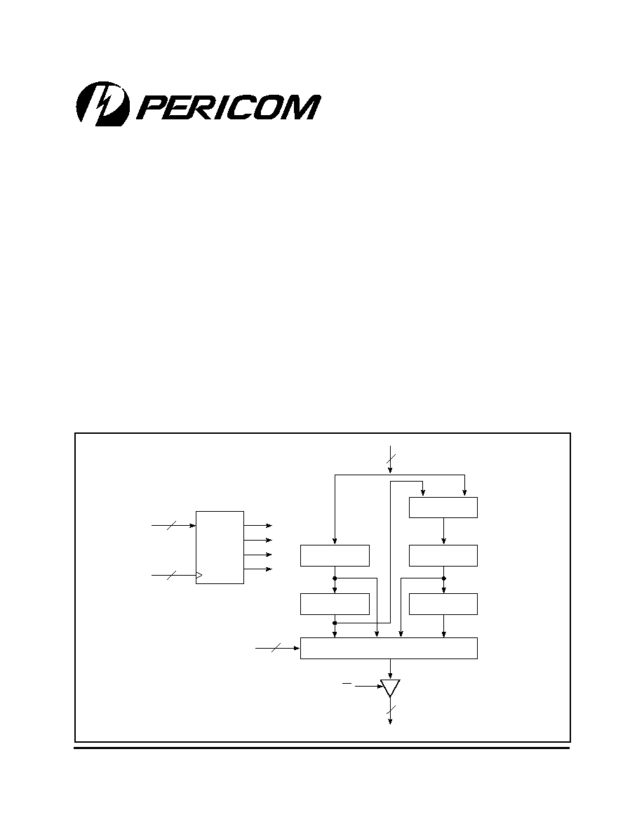
Logic Block Diagram
12345678901234567890123456789012123456789012345678901234567890121234567890123456789012345678901212345678901234567890123
12345678901234567890123456789012123456789012345678901234567890121234567890123456789012345678901212345678901234567890123
PI29FCT520T/2520T
PI29FCT521T
Fast CMOS Multilevel Pipeline Registers
Product Description:
Pericom Semiconductor's PI29FCT series of logic circuits are
pro-duced in the Company's advanced 0.8 micron CMOS
technology, achieving industry leading speed grades.
The PI29FCT520T/2520T and PI29FCT521T are multilevel
pipeline registers containing four 8-bit positive triggered registers
which can be configured as a dual 2-level or a single 4-level
pipeline. These products are designed for use as temporary storage
or for storage delays in pipelined systems.
The PI29FCT521T differs from the PI29FCT520T/2520T only in
the way data is loaded into and between registers in the dual 2-level
operation. When data is entered into the first level (I = 2 or I = 1)
of the PI29FCT520T/2520T, the existing data in the first level is
moved to the second level. In the PI29FCT521T, these instructions
simply overwrite the data in the first level. Transfer of data to the
second level is achieved using the 4-level shift instruction (I = 0)
causing the first level to change. In either part, I = 3 shift
instruction puts the registers on hold.
Device models available upon request.
Product Features:
∑ PI29FCT520T and PI29FCT521T are pinout and
function compatible with IDT29FCT520/521,
QS29FCT520/521 and AMD's Am29520/521
∑ Four 8-bit high-speed registers
∑ Hold, Transfer, and load instructions
∑ Dual two-level or single four-level pipeline operation
∑ TTL input and output levels, reducing problematic
"ground bounce"
∑ High output drive
I
OL
= 48 mA
∑ Extremely low static power (1 mW, typ.)
∑ Industrial operating temperature range: ≠40∞C to +85∞C
∑ FCT (2xxxT) has a 25
series resistor.
∑ Packages available:
≠ 24-pin 300 mil wide plastic DIP (P24)
≠ 24-pin 150 mil wide plastic QSOP (Q24)
≠ 24-pin 150 mil wide plastic TQSOP (R24)
≠ 24-pin 300 mil wide plastic SOIC (S24)
FCT520.pm6
12/18/96, 4:44 PM
1

PI29FCT520/521T/2520T
MULTILEVEL PIPELINE REGISTERS
2
PS2002B 12/10/96
12345678901234567890123456789012123456789012345678901234567890121234567890123456789012345678901212345678901234567890123
12345678901234567890123456789012123456789012345678901234567890121234567890123456789012345678901212345678901234567890123
Product Pin Description
Pin Name
Description
OE
Output Enable Input (Active LOW) for
3-State Output Port
CLK
Clock Input. Enter data into registers on
LOW-to-HIGH transistions
I
0
,I
1
Instruction Inputs
S
0
,S
1
Multiplexer Select. Inputs either register
A1, A2, B1, or B2 data to be avaialbe at the
output ports
Dx
Register Inputs
Yx
Register Outputs
GND
Ground
V
CC
Power
Product Pin Configuration
I
0
I
1
D
0
D
1
D
2
D
3
D
4
D
5
D
6
D
7
CLK
GND
1
2
3
4
5
6
7
8
9
10
11
12
24
23
22
21
20
19
18
17
16
15
14
13
24-PIN
P24
Q24
R24
S24
S1
S0
Register
0
0
B2
0
1
B1
1
0
A2
1
1
A1
Register Selection
PI29FCT520/T2520T Data Loading
A1
A2
B1
B2
A1
A2
B1
B2
A1
A2
B1
B2
DUAL 2-LEVEL
SINGLE 4-LEVEL
I
= 0
I
= 1
I
= 2
NOTE:
I
= 3 FOR HOLD
PI29FCT521T Data Loading
A1
A2
B1
B2
A1
A2
B1
B2
A1
A2
B1
B2
DUAL 2-LEVEL
SINGLE 4-LEVEL
I
= 0
I
= 1
I
= 2
NOTE:
I
= 3 FOR HOLD
V
CC
S
0
S
1
Y
0
Y
1
Y
2
Y
3
Y
4
Y
5
Y
6
Y
7
OE
FCT520.pm6
12/18/96, 4:44 PM
2

PI29FCT520/521T/2520T
MULTILEVEL PIPELINE REGISTERS
3
PS2002B 12/10/96
12345678901234567890123456789012123456789012345678901234567890121234567890123456789012345678901212345678901234567890123
12345678901234567890123456789012123456789012345678901234567890121234567890123456789012345678901212345678901234567890123
Maximum Ratings
(Above which the useful life may be impaired. For user guidelines, not tested.)
Storage Temperature ................................................................. ≠55∞C to +125∞C
Ambient Temperature with Power Applied ................................. -40∞C to +85∞C
Supply Voltage to Ground Potential (Inputs & Vcc Only) .......... ≠0.5V to +7.0V
Supply Voltage to Ground Potential (Outputs & D/O Only) ....... ≠0.5V to +7.0V
DC Input Voltage ......................................................................... ≠0.5V to +7.0V
DC Output Current ................................................................................... 120 mA
Power Dissipation ......................................................................................... 0.5W
Note:
Stresses greater than those listed under
MAXIMUM RATINGS may cause permanent
damage to the device. This is a stress rating
only and functional operation of the device at
these or any other conditions above those
indicated in the operational sections of this
specification is not implied. Exposure to
absolute maximum rating conditions for
extended periods may affect reliability.
Capacitance
(T
A
= 25∞C, f = 1 MHz)
Parameters
(4)
Description
Test Conditions
Typ
Max.
Units
C
IN
Input Capacitance
V
IN
= 0V
6
10
pF
C
OUT
Output Capacitance
V
OUT
= 0V
8
12
pF
Notes:
1. For conditions show as Max. or Min., use appropriate value specified under Electrical Characteristics for the applicable device
type.
2. Typical values are at Vcc = 5.0V, +25∞C ambient and maximum loading.
3. Not more than one output should be shorted at one time. Duration of the test should not exceed one second.
4. This parameter is determined by device characterization but is not production tested.
DC Electrical Characteristics
(Over the Operating Range, T
A
= ≠40∞C to +85∞C, V
CC
= 5V ± 5%)
Parameters
Description
Test Conditions
(1)
Min.
Typ
(2)
Max.
Units
V
OH
Output HIGH Voltage
V
CC
= M
IN
., V
IN
= V
IH
OR
V
IL
I
OH
= ≠15.0 mA
2.4
3.0
V
V
OL
Output LOW Voltage
V
CC
= M
IN
., V
IN
= V
IH
OR
V
IL
I
OL
= 48 mA
0.3
0.50
V
I
OL
= 12 mA (25
series)
0.3
0.50
V
V
IH
Input HIGH Voltage
Guaranteed Logic HIGH Level
2.0
V
V
IL
Input LOW Voltage
Guaranteed Logic LOW Level
0.8
V
I
IH
Input HIGH Current
V
CC
= M
AX
.
V
IN
= V
CC
1
µA
I
IL
Input LOW Current
V
CC
= M
AX
.
V
IN
= GND
≠1
µA
I
OZH
High Impedance
V
CC
= M
AX
.
V
OUT
= 2.7V
1
µA
I
OZL
Output Current
V
OUT
= 0.5V
≠1
µA
V
IK
Clamp Diode Voltage
V
CC
= M
IN
., I
IN
= ≠18 mA
≠0.7
≠1.2
V
I
OS
Short Circuit Current
V
CC
= M
AX
.
(3)
, V
OUT
= GND
≠60
≠120
mA
I
OFF
Power Down Disable
V
CC
= GND, V
OUT
= 4.5V
--
--
100
µA
V
H
Input Hysteresis
200
mV
FCT520.pm6
12/18/96, 4:44 PM
3

PI29FCT520/521T/2520T
MULTILEVEL PIPELINE REGISTERS
4
PS2002B 12/10/96
12345678901234567890123456789012123456789012345678901234567890121234567890123456789012345678901212345678901234567890123
12345678901234567890123456789012123456789012345678901234567890121234567890123456789012345678901212345678901234567890123
Power Supply Characteristics
Parameters Description
Test Conditions
(1)
Min.
Typ
(2)
Max.
Units
I
CC
Quiescent Power
V
CC
= Max.
V
IN
= GND or V
CC
0.1
10
µA
Supply Current
I
CC
Supply Current per
V
CC
= Max.
V
IN
= 3.4V
(3)
0.5
2.0
mA
Input @ TTL HIGH
I
CCD
Supply Current per
V
CC
= Max.,
V
IN
= GND
0.15
0.25
mA/
Input per MHz
(4)
Outputs Open
V
IN
= V
CC
MHz
OE = GND
One Input Toggling
50% Duty Cycle
I
C
Total Power Supply
V
CC
= Max.,
V
IN
= GND
1.5
3.5
(5)
mA
Current
(5)
Outputs Open
V
IN
= V
CC
f
CP
= 10 MH
Z
50% Duty Cycle
OE = GND
V
IN
= 3.4V
2.0
5.5
(5)
One Bit Toggling
V
IN
= GND
f
I
= 5 MH
50% Duty Cycle
V
CC
= Max.,
V
IN
= GND
3.8
7.3
(5)
Outputs Open
V
IN
= V
CC
f
CP
= 10 MH
Z
50% Duty Cycle
OE = GND
V
IN
= 3.4V
6.0
16.3
(5)
Eight Bits Toggling
V
IN
= GND
f
I
= 5 MHz
50% Duty Cycle
Notes:
1. For conditions shown as Max. or Min., use appropriate value specified under Electrical Characteristics for the applicable
device.
2. Typical values are at Vcc = 5.0V, +25∞C ambient.
3. Per TTL driven input (V
IN
= 3.4V, control inputs only); all other inputs at VCC or GND.
4. This parameter is not directly testable, but is derived for use in Total Power Supply characteristics.
5. Values for these conditions are examples of the I
CC
formula. These limits are guAranteed but not tested.
6. I
C
=I
QUIESCENT
+ I
INPUTS
+ I
DYNAMIC
I
C
= I
CC
+
I
CC
D
H
N
T
+ I
CCD
(f
CP
/2 + f
I
N
I
)
I
CC
= Quiescent Current
I
CC
= Power Supply Current for a TTL High Input (V
IN
= 3.4V)
D
H
= Duty Cycle for TTL Inputs High
N
T
= Number of TTL Inputs at D
H
I
CCD
= Dynamic Current Caused by an Input Transition Pair (HLH or LHL)
f
CP
= Clock Frequency for Register Devices (Zero for Non-Register Devices)
f
I
= Input Frequency
N
I
= Number of Inputs at f
I
All currents are in milliamps and all frequencies are in megahertz.
FCT520.pm6
12/18/96, 4:44 PM
4

PI29FCT520/521T/2520T
MULTILEVEL PIPELINE REGISTERS
5
PS2002B 12/10/96
12345678901234567890123456789012123456789012345678901234567890121234567890123456789012345678901212345678901234567890123
12345678901234567890123456789012123456789012345678901234567890121234567890123456789012345678901212345678901234567890123
PI29FCT520T/2520T Switching Characteristics over Operating Range
FCT520AT/2520AT FCT520BT/2520BT
Com.
Com.
Parameters
Description
Conditions
(1)
Min
Max
Min
Max
Unit
t
PLH
Propagation Delay
C
L
= 50 pF
2.0
14.0
2.0
7.5
ns
t
PHL
CLK to Y
X
R
L
= 500
t
PLH
Propagation Delay
2.0
13.0
2.0
7.5
ns
t
PHL
S
0
or S
1
to Y
X
t
SU
Setup Time HIGH
5.0
--
2.5
--
ns
or LOW D
X
to CLK
t
H
Hold Time HIGH
2.0
--
2.0
--
ns
or LOW D
X
to CLK
t
SU
Setup Time HIGH
5.0
--
4.0
--
ns
or LOW I
0
or I
1
to CLK
t
H
Hold Time HIGH
2.0
--
2.0
--
ns
or LOW I
0
or I
1
to CLK
t
PZH
Output Enable Time
1.5
12.0
1.5
7.0
ns
t
PZL
OE to Y
X
t
PHZ
Output Disable Time
(3)
1.5
15.0
1.5
7.5
ns
t
PLZ
OE to Yx
t
W
Clock Pulse Width
(3)
7.0
--
5.5
--
ns
HIGH or LOW
Notes:
1. See test circuit and wave forms.
2. Minimum limits are guaranteed but not tested on Propagation Delays.
3. This parameter is guaranteed but not production tested.
PI29FCT521T Switching Characteristics over Operating Range
FCT521AT
FCT521BT
Com.
Com.
Parameters
Description
Conditions
(1)
Min
Max
Min
Max
Unit
t
PLH
Propagation Delay
C
L
= 50 pF
2.0
14.0
2.0
7.5
ns
t
PHL
CLK to Y
X
R
L
= 500
t
PLH
Propagation Delay
2.0
13.0
2.0
7.5
ns
t
PHL
S
0
or S
1
to Y
X
t
SU
Setup Time HIGH
5.0
--
2.5
--
ns
or LOW D
X
to CLK
t
H
Hold Time HIGH
2.0
--
2.0
--
ns
or LOW D
X
to CLK
t
SU
Setup Time HIGH
5.0
--
4.0
--
ns
or LOW I
0
or I
1
to CLK
t
H
Hold Time HIGH
2.0
--
2.0
--
ns
or LOW I
0
or I
1
to CLK
t
PZH
Output Enable Time
1.5
12.0
1.5
7.0
ns
t
PZL
OE to Yx
t
PHZ
Output Disable Time
(3)
1.5
15.0
1.5
7.5
ns
t
PLZ
OE to Yx
t
W
Clock Pulse Width
(3)
7.0
--
5.5
--
ns
HIGH or LOW
Pericom Semiconductor Corporation
2380 Bering Drive ∑ San Jose, CA 95131 ∑ 1-800-435-2336 ∑ Fax (408) 435-1100 ∑ http://www.pericom.com
FCT520.pm6
12/18/96, 4:44 PM
5