
1
PS8789 09/19/05
Features
∑ 2 Differential Channel, 2:1 Mux/DeMux
∑ PCI Express signal compliance
∑ Low Bit-to-Bit Skew
∑ Low Crosstalk: -60dB@10MHz
∑ Low Off Isolation: -65dB@10MHz
∑ V
CC
Operating Range: +1.5V to +2.0V
∑ ESD Tolerance >2kV HBM
∑ Packaging (Pb-free & Green):
≠ 28 contact TQFN (ZH)
Description
Pericom Semiconductor's PI2PCIE212 is a 4 to 2 differential
channel multiplexer/demultiplexer switch. The PI2PCIE family
of switch solutions is fully compliant with PCI-express signals
at 2.5Gbps. PI2PCIE212 can switch PCI-express signals up to
a maximum length of 16 inches. Due to its low bit-to-bit skew,
high channel-to-channel noise isolation and high bandwidth, this
product is ideal for PCI Express switching.
Application
Switch a PCI-Express lane output between two PCI-Express lane
inputs
Block Diagram
Pin Description
PI2PCIE212
1.8V, PCI Express Compliant, 2 Differential Channel,
2:1 Mux/DeMux Switch w/ Single Enable
A3
A2
A1
A0
1B1
0B1
1B2
0B2
3B1
2B1
3B2
2B2
SEL
Truth Table
Function
SEL
A
n
to
n
B
1
L
A
n
to
n
B
2
H
GND
SEL
V
DD
A0
A1
A2
A3
V
DD
V
DD
GND
0B1
1B1
2B1
3B1
GND
V
DD
0B2
1B2
2B2
3B2
GND
V
DD
GND
V
DD
V
DD
GND
V
DD
GND
1
2
3
4
5
6
7
8
9
10
24
23
22
21
20
19
18
17
16
15
28 27 26 25
11 12 13 14
GND

2
PI2PCIE212
1.8V, PCI Express Compliant, 2 Differential Ch.,
2:1 Mux/DeMux Switch w/ Single Enable
PS8789 09/19/05
DC Electrical Characteristics for Switching over Operating Range
(T
A
= ≠40∞C to +85∞C, V
CC
= 1.5V to 2.0V)
Paramenter
Description
Test Conditions
Min.
Typ.
(2)
Max.
Units
V
IH
Input HIGH Voltage
Guaranteed HIGH level
0.65 x V
CC
-
-
V
V
IL
Input LOW Voltage
Guaranteed LOW level
-0.5
-
0.35 x V
CC
V
IK
Clamp Diode Voltage
V
CC
= Max., I
IN
= ≠18mA
-
-0.7
-1.2
I
IH
Input HIGH Current
V
CC
= Max., V
IN
= V
CC
-
-
±5
A
I
IL
Input LOW Current
V
CC
= Max., V
IN
= GND
-
-
±5
Storage Temperature ......................................... ≠65∞C to +150∞C
Supply Voltage to Ground Potential ....................≠0.5V to +2.5V
DC Input Voltage ..................................................≠0.5V to +V
CC
DC Output Current ........................................................... 120mA
Power Dissipation ................................................................ 0.5W
Note:
Stresses greater than those listed under MAXIMUM RATINGS
may cause permanent damage to the device. This is a stress rating only
and functional operation of the device at these or any other conditions
above those indicated in the operational sections of this specification
is not implied. Exposure to absolute maximum rating conditions for
extended periods may affect reliability.
Maximum Ratings
(Above which useful life may be impaired. For user guidelines, not tested.)

3
PI2PCIE212
1.8V, PCI Express Compliant, 2 Differential Ch.,
2:1 Mux/DeMux Switch w/ Single Enable
PS8789 09/19/05
Dynamic Electrical Characteristics Over the Operating Range
(TA= -40∫ to +85∫C, VCC = 1.8V±10%, GND=0V)
Parameter
Description
Test Conditions
Min.
Typ.
(2)
Max.
Units
X
TALK
Crosstalk
See Fig. 1 for Measurement
Setup,
f = 10 MHz
-60
dB
O
IRR
OFF Isolation
See Fig. 2 for Measurement
Setup,
f = 10 MHz
-65
Notes:
1. Guaranteed by design.
Power Supply Characteristics
Parameters
Description
Test Conditions
(1)
Min.
Typ.
(2)
Max.
Units
I
CC
Quiescent Power Supply Current
V
CC
= Max., V
IN
= GND or V
CC
200
µA
Notes:
1. For Max. or Min. conditions, use appropriate value specified under Electrical Characteristics for the applicable device type.
2. Typical values are at V
CC
= 1.8V, T
A
= 25∞C ambient and maximum loading.
Fig 1. Crosstalk Setup

4
PI2PCIE212
1.8V, PCI Express Compliant, 2 Differential Ch.,
2:1 Mux/DeMux Switch w/ Single Enable
PS8789 09/19/05
Fig 2. Off-isolation setup
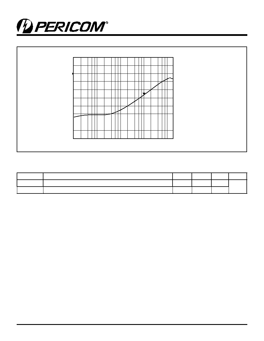
Fig 3. Crosstalk
CH1 A/R log MAG
10 dB/ REF -20 dB
-44.102 dB
100 MHz
Cor
Hld
IF BW 300 Hz
Start 100 kHz
Power 0 dbm
SWP 1.624 sec
STOP 1.8 GHz
Select
Letter
Space
Back
Space
Erase
Title
Done
STOR DEV
[DISK]
Cancel
0
5
PI2PCIE212
1.8V, PCI Express Compliant, 2 Differential Ch.,
2:1 Mux/DeMux Switch w/ Single Enable
PS8789 09/19/05
Notes:
1. For max. or min. conditions, use appropriate value specified under Electrical Characteristics for the applicable device type.
Switching Characteristics
(TA= -40∫ to +85∫C, VCC = 1.8V±10%)
Paramenter
Description
Min.
Typ.
(2)
Max.
Units
tPZH, tPZL Line Enable Time - SEL to AN, BN
0.5
-
8.0
tPHZ, tPLZ Line Disable Time - SEL to AN, BN
0.5
-
4.0
Fig 4. Off Isolation
CH1 A/R log MAG
10 dB/ REF --20 dB
-46.499 dB
100 MHz
Cor
Hld
IF BW 300 Hz
Start 100 kHz
Power 0 dbm
SWP 1.624 sec
STOP 1.8 GHz
Select
Letter
Space
Back
Space
Erase
Title
Done
STOR DEV
[DISK]
Cancel
0