 | –≠–ª–µ–∫—Ç—Ä–æ–Ω–Ω—ã–π –∫–æ–º–ø–æ–Ω–µ–Ω—Ç: PI3B16233 | –°–∫–∞—á–∞—Ç—å:  PDF PDF  ZIP ZIP |
1
PS8171E 09/29/04
12345678901234567890123456789012123456789012345678901234567890121234567890123456789012345678901212345678901234567890123456789012123456789012
12345678901234567890123456789012123456789012345678901234567890121234567890123456789012345678901212345678901234567890123456789012123456789012
12345678901234567890123456789012123456789012345678901234567890121234567890123456789012345678901212345678901234567890123456789012123456789012
Features
∑ 5-ohm Switch Connection Between Two Ports
∑ Nea-Zero Propagation Delay
∑ Fast Switching Speed: 4.5ns (max.)
∑ Ultra -Low Quiescent Power (0.2mA typical)
- ideal for notebook applications.
∑ Industrial Operating Temperature: ≠40∫C to 85∫C
∑ Package (Pb-free & Green available):
- 56-pin 240-mil wide plastic TSSOP(A)
- 56-pin 300- mil wide plastic SSOP (V)
Description
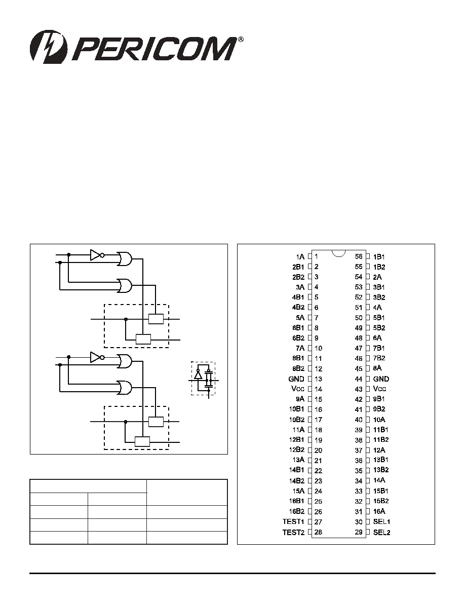
Pericom Semiconductor's PI3B16233 is a 16-bit to 32-bit mux/demux
switch. This device can be used for memory bank interleaving. The
PI3B16233 can be used as two 8-bit to 16-bit multiplexers or as one
16-bit to 32-bit multiplexer.
Two select inputs (SEL1 and SEL2) control the data flow. When the
TEST inputs are asserted HIGH, the A port is connected to both the
B1 and the B2 ports.
PI3B16233
3.3V, 16-Bit to 32-Bit FET
Mux/Demux NanoSwitchTM
Block Diagram
Function Table
Pin Configuration
s
t
u
p
n
I
n
o
i
t
c
n
u
F
L
E
S
T
S
E
T
L
L
1
B
=
A
H
L
2
B
=
A
X
H
2
B
=
A
d
n
a
1
B
=
A
SEL
1
TEST
1
30
1
55
56
27
1A
One of Eight
Channels
1B2
1B1
SEL
2
TEST
2
29
15
41
42
28
9A
One of Eight
Channels
9B2
9B1
A
B
S
SW
SW
SW
SW
SW

PI3B16233
3.3V, 16-Bit to 32-Bit
FET Mux/Demux NanoSwitch
2
PS8171E 09/29/04
12345678901234567890123456789012123456789012345678901234567890121234567890123456789012345678901212345678901234567890123456789012123456789012
Notes:
1. For Max. or Min. conditions, use appropriate value specified under Electrical Characteristics for the applicable device type.
2. Typical values are at V
CC
= 3.3V, T
A
= 25∞C ambient and maximum loading.
3. Measured by the voltage drop between A and B pin at indicated current through the switch. ON resistance is determined
by the lower of the voltages on the two (A,B) pins.
4. This parameter is determined by device characterization but is not production tested.
Capacitance
(T
A
= 25∞C, f = 1 MHz)
Maximum Ratings
(Above which the useful life may be impaired. For user guidelines, not tested.)
Storage Temperature ...................................................... ≠65∞C to +150∞C
Ambient Temperature with Power Applied ...................... ≠40∞C to +85∞C
Supply Voltage Range ....................................................... ≠0.5V to +4.6V
DC Input Voltage ............................................................... ≠0.5V to +4.6V
DC Output Current ........................................................................ 120mA
Power Dissipation ............................................................................. 0.5W
Note:
Stresses greater than those listed under MAXIMUM RAT-
INGS may cause permanent damage to the device. This is a
stress rating only and functional operation of the device at these
or any other conditions above those indicated in the operational
sections of this specification is not implied. Exposure to
absolute maximum rating conditions for extended periods may
affect reliability.
DC Electrical Characteristics
(Over the Operating Range, T
A
= ≠40∞C to +85∞C, V
CC
= 3.0V to 3.6V)
s
r
e
t
e
m
a
r
a
P
n
o
i
t
p
i
r
c
s
e
D
s
n
o
i
t
i
d
n
o
C
t
s
e
T
)
1
(
.
n
i
M
.
p
y
T
)
2
(
.
x
a
M
s
t
i
n
U
V
H
I
e
g
a
tl
o
V
H
G
I
H
t
u
p
n
I
l
e
v
e
L
h
g
i
H
c
i
g
o
L
d
e
e
t
n
a
r
a
u
G
0
.
2
V
V
L
I
e
g
a
tl
o
V
W
O
L
t
u
p
n
I
l
e
v
e
L
w
o
L
c
i
g
o
L
d
e
e
t
n
a
r
a
u
G
5
.
0
≠
8
.
0
I
H
I
t
n
e
r
r
u
C
H
G
I
H
t
u
p
n
I
V
C
C
V
;.
x
a
M
=
N
I
V
=
C
C
1
±
A
µ
I
L
I
t
n
e
r
r
u
C
W
O
L
t
u
p
n
I
V
C
C
V
;.
x
a
M
=
N
I
=
D
N
G
1
±
I
H
Z
O
t
n
e
r
r
u
C
t
u
p
t
u
O
e
c
n
a
d
e
p
m
I
h
g
i
H
0
B
,
A
V
C
C
1
±
V
K
I
e
g
a
tl
o
V
e
d
o
i
D
p
m
a
l
C
V
C
C
I
,
n
i
M
=
N
I
A
m
8
1
≠
=
7
.
0
≠
2
.
1
≠
V
R
N
O
e
c
n
a
t
s
i
s
e
R
N
O
h
c
ti
w
S
)
3
(
V
C
C
V
,.
n
i
M
=
N
I
I
,
V
0
.
0
=
N
O
A
m
4
6
r
o
A
m
8
4
=
V
C
C
V
,.
n
i
M
=
N
I
I
,
V
4
.
2
=
N
O
A
m
5
1
=
5
0
1
8
5
1
s
r
e
t
e
m
a
r
a
P
)
5
(
n
o
i
t
p
i
r
c
s
e
D
s
n
o
i
t
i
d
n
o
C
t
s
e
T
.
p
y
T
s
t
i
n
U
C
N
I
e
c
n
a
ti
c
a
p
a
C
t
u
p
n
I
V
N
I
V
0
=
0
.
3
F
p
C
N
O
n
O
h
c
ti
w
S
,
e
c
n
a
ti
c
a
p
a
C
B
/
A
0
.
5
2

PI3B16233
3.3V, 16-Bit to 32-Bit
FET Mux/Demux NanoSwitch
3
PS8171E 09/29/04
12345678901234567890123456789012123456789012345678901234567890121234567890123456789012345678901212345678901234567890123456789012123456789012
12345678901234567890123456789012123456789012345678901234567890121234567890123456789012345678901212345678901234567890123456789012123456789012
Power Supply Characteristics
Notes:
1. For Max. or Min. conditions, use appropriate value specified under Electrical Characteristics for the applicable device.
2. Typical values are at V
CC
= 3.3V, +25∞C ambient.
3. Per TTL driven input (control inputs only); A and B pins do not contribute to I
CC
.
4. This current applies to the control inputs only and represent the current required to switch internal capacitance at the specified frequency.
The A and B inputs generate no significant AC or DC currents as they transition. This parameter is not tested, but is guaranteed by design.
Switching Characteristics over Operating Range
Notes:
1. See test circuit and waveforms.
2. This parameter is guaranteed but not tested on Propagation Delays.
3. The bus switch contributes no propagational delay other than the RC delay of the ON resistance of the switch and the load capacitance. The
time constant for the switch alone is of the order of 0.25ns for 50pF load. Since this time constant is much smaller than the rise/fall times of
typical driving signals, it adds very little propagational delay to the system. Propagational
delay of the bus switch when used in a system is determined by the driving circuit on the driving side of the switch and its interaction with
the load on the driven side.
s
r
e
t
e
m
a
r
a
P
n
o
i
t
p
i
r
c
s
e
D
s
n
o
i
t
i
d
n
o
C
t
s
e
T
)
1
(
.
n
i
M
p
y
T
)
2
(
.
x
a
M
s
t
i
n
U
I
C
C
r
e
w
o
P
t
n
e
c
s
e
i
u
Q
t
n
e
r
r
u
C
y
l
p
p
u
S
V
C
C
.
x
a
M
=
V
N
I
D
N
G
=
V
r
o
C
C
0
1
A
µ
I
C
C
t
u
p
n
I
r
e
p
t
n
e
r
r
u
C
y
l
p
p
u
S
h
g
i
H
L
T
T
@
V
C
C
.
x
a
M
=
V
N
I
)
3
(
V
0
.
3
=
0
5
7
I
D
C
C
r
e
p
t
n
e
r
r
u
C
y
l
p
p
u
S
z
H
M
r
e
p
t
u
p
n
I
)
4
(
V
C
C
n
e
p
O
n
i
P
B
&
A
.
x
a
M
=
g
n
il
g
g
o
T
t
u
p
n
I
l
o
r
t
n
o
C
e
l
c
y
C
y
t
u
D
%
0
5
5
2
.
0
/
A
m
z
H
M
s
r
e
t
e
m
a
r
a
P
n
o
i
t
p
i
r
c
s
e
D
s
n
o
i
t
i
d
n
o
C
(1)
.
m
o
C
.
x
a
M
.
n
i
M
s
t
i
n
U
t
H
L
P
t
L
H
P
y
a
l
e
D
n
o
it
a
g
a
p
o
r
P
)
3
,
2
(
x
A
o
t
x
B
,
x
B
o
t
x
A
C
L
,
F
p
0
5
=
R
L
0
0
5
=
5
2
.
0
s
n
t
H
Z
P
t
L
Z
P
e
m
i
T
e
l
b
a
n
E
s
u
B
L
E
S
X
x
B
r
o
x
A
o
t
C
L
R
,
F
p
0
5
=
L
0
0
5
=
,
R
0
0
5
=
1
5
.
4
t
Z
H
P
t
Z
L
P
e
m
i
T
e
l
b
a
s
i
D
s
u
B
L
E
S
X
x
B
r
o
x
A
o
t
C
L
R
,
F
p
0
5
=
L
0
0
5
=
1
0
.
5

PI3B16233
3.3V, 16-Bit to 32-Bit
FET Mux/Demux NanoSwitch
4
PS8171E 09/29/04
12345678901234567890123456789012123456789012345678901234567890121234567890123456789012345678901212345678901234567890123456789012123456789012
.002
.006
SEATING PLANE
.007
.011
.004
.008
1
56
.236
.244
0.50
0.17
0.27
0.05
0.15
0.09
0.20
X.XX
X.XX
DENOTES DIMENSIONS
IN MILLIMETERS
.018
.030
0.45
0.75
.047
Max.
1.20
6.0
6.2
.547
.555
13.9
14.1
.319
8.1
.0197
BSC
BSC
Packaging Mechanical: 56-Pin TSSOP (A)
0.25
0.20
.025 BSC
0.635
.008
.008
.016
0-8∞
0.20
0.40
.110 2.79
.010
Gauge Plane
.291
.299
X.XX
X.XX
DENOTES DIMENSIONS
IN MILLIMETERS
7.39
7.59
.396
.416
10.06
10.56
.02
.04
0.51
1.01
.015
.025
0.381
0.635
.720
.730
18.29
18.54
.008
.0135
0.20
0.34
1
56
x 45∞
Nom.
Max
Packaging Mechanical: 56-Pin SSOP (V)
PI3B16233
3.3V, 16-Bit to 32-Bit
FET Mux/Demux NanoSwitch
5
PS8171E 09/29/04
12345678901234567890123456789012123456789012345678901234567890121234567890123456789012345678901212345678901234567890123456789012123456789012
12345678901234567890123456789012123456789012345678901234567890121234567890123456789012345678901212345678901234567890123456789012123456789012
Applications Information
Logic Inputs
The logic control inputs can be driven up to +3.6V regardless of the supply voltage. For example, given a + 3.3V supply, IN may be
driven low to 0V and high to 3.6V. Driving IN Rail-to-RailÆ minimizes power consumption.
Power-Supply Sequencing and Hot-Plug Information
Proper power-supply sequencing is recommended for all CMOS devices. Always apply V
CC
and GND before applying signals to
input/output or control pins.
Rail-to-Rail is a registeredtrademark of Nippon Motorola, Ltd.
Notes:
1. Thermal characteristics can be found on the company web site at www.pericom.com/packaging/
Ordering Information
Ordering Code
Package Code
Package Type
PI3B16233A
A
56-pin 240-mil wide TSSOP
PI3B16233AE
A
Pb-free & Green, 56-pin 240-mil wide TSSOP
PI3B16233V
V
56-pin 300-mil wide SSOP
PI3B16233VE
V
Pb-free & Green, 56-pin 300-mil wide SSOP
Pericom Semiconductor Corporation ∑ 1-800-435-2336 ∑ www.pericom.com