
1
PS8452C 03/13/01
12345678901234567890123456789012123456789012345678901234567890121234567890123456789012345678901212345678901234567890123456789012123456789012
12345678901234567890123456789012123456789012345678901234567890121234567890123456789012345678901212345678901234567890123456789012123456789012
Truth Table
(1)
Note:
1. H = High Voltage Level
L = Low Voltage Level
Hi-Z = High Impedance
Pin Name
Description
1
OE,
2
OE
Bus Enable Inputs (Active LOW)
1
A
1
-
1
A
10
,
2
A
1
-
2
A
10
Bus A
1
B
1
-
1
B
10
,
2
B
1
-
2
B
10
Bus B
Product Pin Description
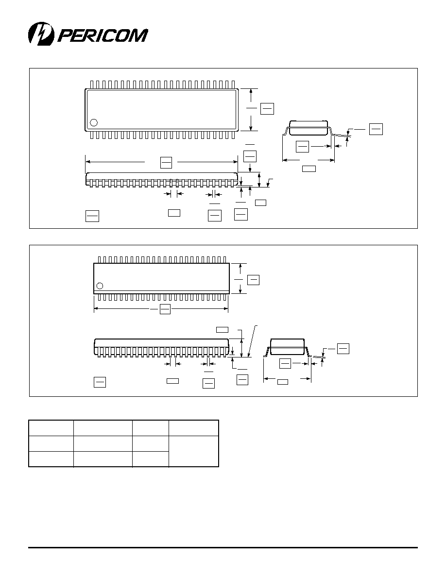
Product Pin Configuration
PI3C16210
3.3V, High Bandwidths 20-Bit,
2-Port Bus Switch
Product Features
Near-zero propagation delay
5-Ohm switch connects inputs to outputs
Direct bus connection when switch is ON
32X384 function with flow through pinout makes
board layout easier
Ultra-low quiescent power (0.2mA typical)
ideally suited for notebook applications
Industrial operating temperature: 40�C to +85�C
Packages available:
48-pin 173-mil wide plastic TVSOP (K)
48-pin 240-mil wide plastic TSSOP (A)
Product Description
Pericom Semiconductors PI3C series of Bus Switch circuits are
produced using the Companys advanced submicron CMOS
technology, achieving industry leading speed.
The PI3C16210 is configured as a 20-bit, 2-port bus switch designed
with a low ON resistance (5 Ohm) allowing inputs to be connected
directly to outputs. The bus switch creates no additional
propagational delay or additional ground bounce noise. The switch
is turned ON by the Bus Enable (xOE) input signal.
Logic Block Diagram
s
t
u
p
n
I
s
t
u
p
t
u
O
/
s
t
u
p
n
I
1
E
O
2
E
O
1
,
A
1
B
2
,
A
2
B
L
L
1
=
A
1
B
2
=
A
2
B
L
H
1
=
A
1
B
Z
H
L
Z
2
=
A
2
B
H
H
Z
Z
1
OE
1
A
10
1
A
1
1
B
10
1
B
1
2
OE
2
A
10
2
A
1
2
B
10
2
B
1
NC
1
A
1
1
A
2
1
A
3
1
A
4
1
A
5
1
A
6
GND
1
A
7
1
A
8
1
A
9
1
A
10
2
A
1
2
A
2
V
CC
2
A
3
GND
2
A
4
2
A
5
2
A
6
2
A
7
2
A
8
2
A
9
2
A
10
1
2
3
4
5
6
7
8
9
10
11
12
13
14
15
16
17
18
19
20
21
22
23
24
1
OE
2
OE
1
B
1
1
B
2
1
B
3
1
B
4
1
B
5
GND
1
B
6
1
B
7
1
B
8
1
B
9
1
B
10
2
B
1
2
B
2
2
B
3
GND
2
B
4
2
B
5
2
B
6
2
B
7
2
B
8
2
B
9
2
B
10
48
47
46
45
44
43
42
41
40
39
38
37
36
35
34
33
32
31
30
29
28
27
26
25
48-Pin
A, K
2
PS8452C 03/13/01
12345678901234567890123456789012123456789012345678901234567890121234567890123456789012345678901212345678901234567890123456789012123456789012
12345678901234567890123456789012123456789012345678901234567890121234567890123456789012345678901212345678901234567890123456789012123456789012
PI3C16210
3.3V, High Bandwidth , 20-Bit, 2-Port Bus Switch
Storage Temperature............................................................. 65�C to +150�C
Ambient Temperature with Power Applied .............................. 40�C to +85�C
Supply Voltage to Ground Potential (Inputs & V
CC
Only) ........ 0.5V to +4.6V
Supply Voltage to Ground Potential (Outputs & D/O Only) ...... 0.5V to +4.6V
DC I/O Voltage ........................................................................... 0.5V to +5.5V
DC Output Current .................................................................................120mA
Power Dissipation .................................................................................... 0.5W
Note:
Stresses greater than those listed under MAXIMUM
RATINGS may cause permanent damage to the
device. This is a stress rating only and functional
operation of the device at these or any other condi-
tions above those indicated in the operational sec-
tions of this specification is not implied. Exposure to
absolute maximum rating conditions for extended
periods may affect reliability.
Notes:
1. For Max. or Min. conditions, use appropriate value specified under Electrical Characteristics for the applicable device type.
2. Typical values are at V
CC
= 3.3V, T
A
= 25�C ambient and maximum loading.
3. Not more than one output should be shorted at one time. Duration of the test should not exceed one second.
4. Measured by the voltage drop between A and B pin at indicated current through the switch. ON resistance is determined by the
lower of the voltages on the two (A,B) pins.
5. This parameter is determined by device characterization but is not production tested.
Maximum Ratings
(Above which the useful life may be impaired. For user guidelines, not tested.)
DC Electrical Characteristics
(Over the Operating Range, T
A
= 40�C to +85�C, V
CC
= 3.3V �10%)
Capacitance
(T
A
= 25�C f = 1 MHz)
s
r
e
t
e
m
a
r
a
P
n
o
it
p
i
r
c
s
e
D
s
n
o
it
i
d
n
o
C
t
s
e
T
)
1
(
.
n
i
M
.
p
y
T
)
2
(
.
x
a
M
s
ti
n
U
V
H
I
e
g
a
tl
o
V
H
G
I
H
t
u
p
n
I
l
e
v
e
L
H
G
I
H
ci
g
o
L
d
e
e
t
n
a
r
a
u
G
0
.
2
V
V
L
I
e
g
a
tl
o
V
W
O
L
t
u
p
n
I
l
e
v
e
L
W
O
L
ci
g
o
L
d
e
e
t
n
a
r
a
u
G
5
.
0
8
.
0
I
H
I
t
n
e
rr
u
C
H
G
I
H
t
u
p
n
I
V
C
C
V
,.
x
a
M
=
N
I
V
=
C
C
1
�
A
�
I
L
I
t
n
e
rr
u
C
W
O
L
t
u
p
n
I
V
C
C
V
,.
x
a
M
=
N
I =
D
N
G
1
�
I
Z
O
)
3
(
t
u
p
t
u
O
e
c
n
e
d
e
p
m
I
-
h
g
i
H
t
n
e
rr
u
C
0
B
,
A
V
C
C
1
�
V
K
I
e
g
a
tl
o
V
e
d
o
i
d
p
m
al
C
V
C
C
I
,.
n
i
M
=
N
I
A
m
8
1
=
3
7
.
0
2
.
1
V
R
N
O
e
c
n
a
t
si
s
e
R
n
O
h
c
ti
w
S
)
4
(
V
C
C
V
,.
n
i
M
=
N
I
V
0
.
0
=
I
N
O
A
m
4
6
r
o
A
m
8
4
=
5
.
6
5
.
8
V
C
C
V
,.
n
i
M
=
N
I
V
4
.
2
=
I
N
O
A
m
5
1
=
0
1
5
1
s
r
e
t
e
m
a
r
a
P
)
5
(
n
o
it
p
i
r
c
s
e
D
s
n
o
it
i
d
n
o
C
t
s
e
T
.
p
y
T
s
ti
n
U
C
N
I
e
c
n
a
ti
c
a
p
a
C
t
u
p
n
I
V
N
I
V
0
=
5
.
3
F
p
C
F
F
O
ff
O
h
c
ti
w
S
,
e
c
n
a
ti
c
a
p
a
C
B
/
A
0
.
4
C
N
O
n
O
h
c
ti
w
S
,
e
c
n
a
ti
c
a
p
a
C
B
/
A
0
.
8
3
PS8452C 03/13/01
12345678901234567890123456789012123456789012345678901234567890121234567890123456789012345678901212345678901234567890123456789012123456789012
12345678901234567890123456789012123456789012345678901234567890121234567890123456789012345678901212345678901234567890123456789012123456789012
PI3C16210
3.3V, High Bandwidth , 20-Bit, 2-Port Bus Switch
s
r
e
t
e
m
a
r
a
P
n
o
it
p
i
r
c
s
e
D
s
n
o
it
i
d
n
o
C
)
1
(
.
m
o
C
s
ti
n
U
.
n
i
M
.
x
a
M
t
H
L
P
t
L
H
P
y
al
e
D
n
o
it
a
g
o
p
o
r
P
)
3
,
2
(
x
A
o
t
x
B
,
x
B
o
t
x
A
C
L
F
p
0
5
=
R
L
0
0
5
=
5
2
.
0
s
n
t
H
Z
P
t
L
Z
P
e
m
i
T
el
b
a
n
E
s
u
B
x
B
r
o
x
A
o
t
x
E
B
C
L
F
p
0
5
=
R
L
0
0
5
=
0
0
5
=
R
5
.
1
5
.
6
t
Z
H
P
t
Z
L
P
e
m
i
T
el
b
a
si
D
s
u
B
x
B
r
o
x
A
o
t
x
E
B
5
.
1
5
.
5
PI3C16210 Switching Characteristics over Operating Range
Notes:
1. For Max. or Min. conditions, use appropriate value specified under Electrical Characteristics for the applicable device.
2. Typical values are at V
CC
= 3.3V, +25�C ambient.
3. Per TTL driven input (control inputs only); A and B pins do not contribute to I
CC
.
Power Supply Characteristics
Notes:
1. See test circuit and waveforms.
2. This parameter is guaranteed but not tested on Propagation Delays.
3. The bus switch contributes no propagational delay other than the RC delay of the ON resistance of the switch and the load
capacitance. The time constant for the switch alone is of the order of 0.25ns for 50pF load. Since this time constant is much smaller
than the rise/fall times of typical driving signals, it adds very little propagational delay to the system. Propagational delay of the
bus switch when used in a system is determined by the driving circuit on the driving side of the switch and its interaction with the
load on the driven side.
Pericom Semiconductor Corporation
2380 Bering Drive San Jose, CA 95131 1-800-435-2336 Fax (408) 435-1100 http://www.pericom.com
s
r
e
t
e
m
a
r
a
P
n
o
it
p
i
r
c
s
e
D
s
n
o
it
i
d
n
o
C
t
s
e
T
)
1
(
.
n
i
M
.
p
y
T
)
2
(
.
x
a
M
s
ti
n
U
I
C
C
t
n
e
rr
u
C
y
l
p
p
u
S
r
e
w
o
P
t
n
e
c
s
ei
u
Q
V
C
C
,.
x
a
M
=
V
N
I
V
r
o
D
N
G
=
C
C
0
6
2
0
5
8
A
�
I
C
C
H
G
I
H
L
T
T
@
t
u
p
n
I
r
e
p
t
n
e
rr
u
C
y
l
p
p
u
S
V
C
C
,.
x
a
M
=
V
N
I =
V
0
.
3
)
3
(
0
5
7
4
PS8452C 03/13/01
12345678901234567890123456789012123456789012345678901234567890121234567890123456789012345678901212345678901234567890123456789012123456789012
12345678901234567890123456789012123456789012345678901234567890121234567890123456789012345678901212345678901234567890123456789012123456789012
PI3C16210
3.3V, High Bandwidth , 20-Bit, 2-Port Bus Switch
Pericom Semiconductor Corporation
2380 Bering Drive San Jose, CA 95131 1-800-435-2336 Fax (408) 435-1100 http://www.pericom.com
Ordering Information
48-Pin TVSOP (K) Package
t
r
a
P
e
g
a
k
c
a
P
-
n
i
P
h
t
d
i
W
e
r
u
t
a
r
e
p
m
e
T
A
0
1
2
6
1
C
3
I
P
)
A
(
P
O
S
S
T
-
8
4
li
m
-
0
4
2
C
�
5
8
o
t
C
�
0
K
0
1
2
6
1
C
3
I
P
)
K
(
P
O
S
V
T
-
8
4
li
m
-
3
7
1
48-Pin TSSOP (A) Package
.378
.386
.047
.031
.041
SEATING
PLANE
.0051
.009
.016
BSC
1
48
.169
.177
9.60
9.80
4.30
4.50
0.40
0.13
0.23
0.80
1.05
X.XX
X.XX
DENOTES DIMENSIONS
IN MILLIMETERS
.002
.006
0.05
0.15
.0035
.008
0.09
0.20
.018
.030
0.45
0.75
.252
BSC
6.4
Max.
1.20
.236
.244
.488
.496
.002
.006
SEATING PLANE
.007
.010
.0197
BSC
.004
.008
.319
1
48
12.4
12.6
6.0
6.2
0.50
0.17
0.27
8.1
0.05
0.15
0.09
0.20
X.XX
X.XX
DENOTES DIMENSIONS
IN MILLIMETERS
.018
.030
0.45
0.75
.047
1.20 Max
BSC