
1
PS8429B 12/10/99
NC
1
2
3
4
5
6
7
8
9
GND
10
11
12
13
14
15
16
17
18
19
20
GND
BE1
80
79
78
77
76
75
V
CC
74
73
72
71
70
69
68
67
66
65
64
63
62
B
15
61
A
0
A
1
A
2
A
3
A
4
A
5
A
6
A
7
NC
A
8
A
9
A
10
A
11
A
12
A
13
A
14
A
15
B
14
B
13
B
12
B
11
B
10
B
9
B
8
BE2
V
CC
B
0
B
1
B
2
B
3
B
4
B
5
B
6
B
7
NC
21
22
23
24
25
26
27
28
29
GND
30
31
32
33
34
35
36
37
38
39
40
GND
BE3
60
59
58
57
56
55
V
CC
54
53
52
51
50
49
48
47
46
45
44
43
42
B
31
41
A
16
A
17
A
18
A
19
A
20
A
21
A
22
A
23
NC
A
24
A
25
A
26
A
27
A
28
A
29
A
30
A
31
B
30
B
29
B
28
B
27
B
26
B
25
B
24
BE4
V
CC
B
16
B
17
B
18
B
19
B
20
B
21
B
22
B
23
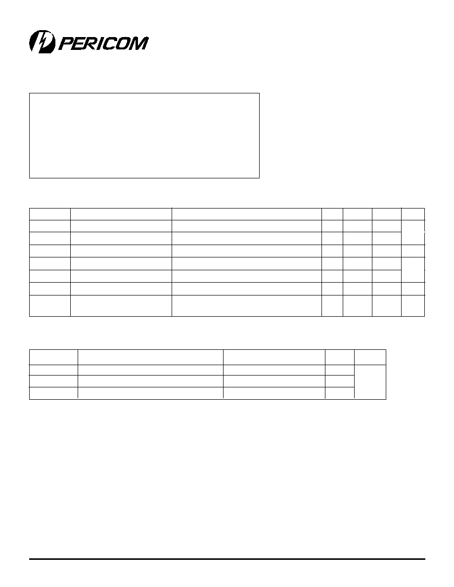
Product Description
Pericom Semiconductors PI3C series of logic circuits are produced
using the Companys advanced submicron CMOS technology,
achieving industry leading performance.
The PI3C34X245 is a 2.5V or 3.3V, 32-bit, 2-port bus switch designed
with a low ON resistance (5
) allowing inputs to be connected
directly to outputs. The bus switch creates no additional propagational
delay or additional ground bounce noise. The switches are turned
ON by the Bus Enable (BE) input signal. It is very useful in switching
signals that have high bandwidth (>400 MHz).
Logic Block Diagram
Product Pin Description
Pin Name
Description
BEn
Bus Enable Input (Active LOW)
A0 A31
Bus A
B0 B31
Bus B
Product Pin Configuration
Product Features
Near zero propagation delay
5
switches connect inputs to outputs
2.5V Supply Voltage Operation
Permits Hot Insertion
5V I/O Tolerant
High Bandwidth Operation (>400 MHz)
Packages available:
80-pin 150 mil wide plastic BQSOP (B)
80-Pin
B
*-
)%
)
*%
*
*-
)#
)&
*#
*&
*-
!
) !
)$
* !
*$
*-
"
)!
) "
*!
* "
PI3C34X245
2.5V/3.3V, High Bandwidth, Hot Insertion
32-Bit, 2-Port, Bus Switch
12345678901234567890123456789012123456789012345678901234567890121234567890123456789012345678901212345678901234567890123456789012123456789012
12345678901234567890123456789012123456789012345678901234567890121234567890123456789012345678901212345678901234567890123456789012123456789012
PI3C34X245
2.5V/3.3V, High Bandwidth,
Hot Insertion, 32-Bit, 2-Port, Bus Switch
2
PS8429B 12/10/99
12345678901234567890123456789012123456789012345678901234567890121234567890123456789012345678901212345678901234567890123456789012123456789012
12345678901234567890123456789012123456789012345678901234567890121234567890123456789012345678901212345678901234567890123456789012123456789012
12345678901234567890123456789012123456789012345678901234567890121234567890123456789012345678901212345678901234567890123456789012123456789012
12345678901234567890123456789012123456789012345678901234567890121234567890123456789012345678901212345678901234567890123456789012123456789012
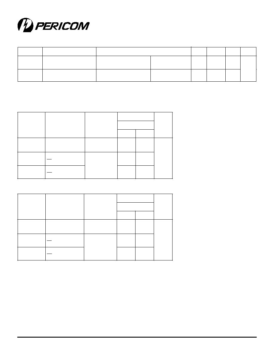
DC Electrical Characteristics
(Over Operating Range, T
A
= ≠40∞C to +85∞C, V
CC
= 3.3V ±10%)
Parameters Description
Test Conditions
(1)
Min.
Typ.
(2)
Max.
Units
V
IH
Input HIGH Voltage
Guaranteed Logic HIGH Level
2.0
V
IL
Input LOW Voltage
Guaranteed Logic LOW Level
≠0.5
0.8
I
IH
Input HIGH Current
V
CC
= Max., V
IN
= V
CC
±1
I
IL
Input LOW Current
V
CC
= Max., V
IN
= GND
±1
µA
I
OZH
High Impedance Output Current
0
A, B
V
CC
±1
V
IK
Clamp Diode Voltage
V
CC
= Min., I
IN
= ≠18mA
≠0.73
≠1.2
V
R
ON
Switch On Resistance
(3)
V
CC
= Min., V
IN
= 0.0V, I
ON
= 48mA
5
7
V
CC
= Min., V
IN
= 2.4V, I
ON
= 15mA
8
15
Storage Temperature ........................................................65∞C to +150∞C
Ambient Temperature with Power Applied ......................... 40∞C to +85∞C
Supply Voltage to Ground Potential (Inputs & V
CC
Only) ........0.5V to +4.6V
Supply Voltage to Ground Potential (Outputs & D/O Only) ......0.5V to +4.6V
DC Input Voltage .................................................................. 0.5V to +5.5V
DC Output Current ............................................................................ 120mA
Power Dissipation ................................................................................ 0.5W
Note:
Stresses greater than those listed under MAXIMUM
RATINGS may cause permanent damage to the
device. This is a stress rating only and functional
operation of the device at these or any other conditions
above those indicated in the operational sections of
this specification is not implied. Exposure to absolute
maximum rating conditions for extended periods may
affect reliability.
Maximum Ratings
(Above which the useful life may be impaired. For user guidelines, not tested.)
Parameters
(4)
Description
Test Conditions
Typ.
Units
C
IN
Input Capacitance
V
IN
= 0V
3.5
C
OFF
A/B Capacitance, Switch Off
V
IN
= 0V
5.0
pF
C
ON
A/B Capacitance, Switch On
V
IN
= 0V
10.0
Notes:
1. For Max. or Min. conditions, use appropriate value specified under Electrical Characteristics for the applicable device type.
2. Typical values are at V
CC
= 3.3V, T
A
= 25∞C ambient and maximum loading.
3. Measured by the voltage drop between A and B pin at indicated current through the switch. ON resistance is determined
by the lower of the voltages on the two (A,B) pins.
4. This parameter is determined by device characterization but is not production tested.
V
Capacitance
(T
A
= 25∞C, f = 1 MHz)
PI3C34X245
2.5V/3.3V, High Bandwidth,
Hot Insertion, 32-Bit, 2-Port, Bus Switch
3
PS8429B 12/10/99
12345678901234567890123456789012123456789012345678901234567890121234567890123456789012345678901212345678901234567890123456789012123456789012
12345678901234567890123456789012123456789012345678901234567890121234567890123456789012345678901212345678901234567890123456789012123456789012
12345678901234567890123456789012123456789012345678901234567890121234567890123456789012345678901212345678901234567890123456789012123456789012
12345678901234567890123456789012123456789012345678901234567890121234567890123456789012345678901212345678901234567890123456789012123456789012
Power Supply Characteristics
Parameters Description
Test Conditions
(1)
Min.
Typ.
(2)
Max.
Units
I
CC
Quiescent Power
V
CC
= Max.
V
IN
= GND or V
CC
1.0
2.0
Supply Current
I
CC
Supply Current per
V
CC
= Max.
V
IN
= 3.0V
(3)
2.5
Input HIGH
Notes:
1. For Max. or Min. conditions, use appropriate value specified under Electrical Characteristics for the applicable device.
2. Typical values are at V
CC
= 3.3V, +25∞C ambient.
3. Per driven input (control input only); A and B pins do not contribute to
I
CC
.
Switching Characteristics over 3.3V Operating Range
mA
s
r
e
t
e
m
a
r
a
P
n
o
it
p
ir
c
s
e
D
s
n
o
it
i
d
n
o
C
5
4
2
X
4
3
C
3
1
P
s
ti
n
U
.
m
o
C
.
n
i
M
.
x
a
M
t
H
L
P
t
L
H
P
y
al
e
D
n
o
it
a
g
a
p
o
r
P
)
3
,
2
(
x
B
o
t
x
A
C
L
F
p
0
5
=
R
L
0
0
5
=
5
2
.
0
s
n
t
H
Z
P
t
L
Z
P
e
m
i
T
el
b
a
n
E
s
u
B
x
B
r
o
x
A
o
t
E
B
C
L
F
p
0
5
=
R
L
0
0
5
=
0
0
5
=
R
5
.
1
8
.
9
t
Z
H
P
t
Z
L
P
e
m
i
T
el
b
a
si
D
s
u
B
x
B
r
o
x
A
o
t
E
B
5
.
1
3
.
8
Switching Characteristics over 2.5V Operating Range
s
r
e
t
e
m
a
r
a
P
n
o
it
p
ir
c
s
e
D
s
n
o
it
i
d
n
o
C
5
4
2
X
4
3
C
3
1
P
s
ti
n
U
.
m
o
C
.
n
i
M
.
x
a
M
t
H
L
P
t
L
H
P
y
al
e
D
n
o
it
a
g
a
p
o
r
P
)
3
,
2
(
x
B
o
t
x
A
C
L
F
p
0
5
=
R
L
0
0
5
=
5
2
.
0
s
n
t
H
Z
P
t
L
Z
P
e
m
i
T
el
b
a
n
E
s
u
B
x
B
r
o
x
A
o
t
E
B
C
L
F
p
0
5
=
R
L
0
0
5
=
0
0
5
=
R
5
.
1
5
.
6
t
Z
H
P
t
Z
L
P
e
m
i
T
el
b
a
si
D
s
u
B
x
B
r
o
x
A
o
t
E
B
5
.
1
5
.
5
Notes:
1. See test circuit and waveforms.
2. This parameter is guaranteed but not tested on Propagation Delays.
3. The bus switch contributes no propagational delay other than the RC delay of the ON
resistance of the switch and the load capacitance. The time constant for the switch alone
is of the order of 0.25ns for 50pF load. Since this time constant is much smaller than the rise/
fall timesof typical driving signals, it adds very little propagational delay to the system.
Propagational delay of the bus switch when used in a system is determined by the driving
circuit on the driving side of the switch and its interaction with the load on the driven side.

PI3C34X245
2.5V/3.3V, High Bandwidth,
Hot Insertion, 32-Bit, 2-Port, Bus Switch
4
PS8429B 12/10/99
12345678901234567890123456789012123456789012345678901234567890121234567890123456789012345678901212345678901234567890123456789012123456789012
12345678901234567890123456789012123456789012345678901234567890121234567890123456789012345678901212345678901234567890123456789012123456789012
12345678901234567890123456789012123456789012345678901234567890121234567890123456789012345678901212345678901234567890123456789012123456789012
12345678901234567890123456789012123456789012345678901234567890121234567890123456789012345678901212345678901234567890123456789012123456789012
t
r
a
P
e
g
a
k
c
a
P
-
n
i
P
s
n
o
i
s
n
e
m
i
D
B
5
4
2
X
4
3
C
3
I
P
)
B
(
P
O
S
Q
B
-
0
8
C
∞
5
8
+
o
t
C
∞
0
4
4.0
2.0
0.0
0.0
1.0
2.0
3.0
4.0
5.0
V
OUT
, (V)
VIN, (V)
VCC =
3.3V
3.1V
2.9V
2.7V
2.5V
2.3V
3.6V
3.8V
3.4V
3.2V
3.0V
2.8V
Output Voltage vs. Input Voltage over Various Supply Voltages
Ordering Information
Pericom Semiconductor Corporation
2380 Bering Drive ∑ San Jose, CA 95131 ∑ 1-800-435-2336 ∑ Fax (408) 435-1100 ∑ http://www.pericom.com