 | –≠–ª–µ–∫—Ç—Ä–æ–Ω–Ω—ã–π –∫–æ–º–ø–æ–Ω–µ–Ω—Ç: PI3L100L | –°–∫–∞—á–∞—Ç—å:  PDF PDF  ZIP ZIP |

1
PS8504 11/13/00
Logic Block Diagram
12345678901234567890123456789012123456789012345678901234567890121234567890123456789012345678901212345678901234567890123456789012123456789012
12345678901234567890123456789012123456789012345678901234567890121234567890123456789012345678901212345678901234567890123456789012123456789012
12345678901234567890123456789012123456789012345678901234567890121234567890123456789012345678901212345678901234567890123456789012123456789012
16-Pin Product Configuration
E
S
YA
YB
YC
YD
Function
H
X
Hi-Z Hi-Z Hi-Z Hi-Z
Disable
L
L
IA0 IB0 IC0 ID0
S = 0
L
H
IA1
IB1
IC1
ID1
S = 1
Truth Table
(1)
Note:
1. H = High Voltage Level
L = Low Voltage Level
Product Pin Description
Pin Name
Description
IAn-IDn
Data Inputs
S
Select Inputs
E
Enable
YA-YD
Data Outputs
GND
Ground
V
CC
Power
PI3L100
3.3V, Wide Bandwidth Quad 2:1
Mux/Demux LanSwitch
Features
∑ Replaces mechanical relays
∑ High-performance, low-cost solution for switching
between different LAN signals
∑ Ultra-low quiescent power (0.1µA typical)
∑ Low crosstalk: ≠90dB @ 30 MHz
∑ Low insertion loss or on-resistance: 3
typical
∑ Single supply operation: 3.3V
∑ Off isolation: ≠45dB @ 30 MHz
∑ Wide bandwidth data rates > 200 MHz
∑ Packages available:
≠ 16-pin 150 mil wide plastic QSOP (Q)
≠ 16-pin 173 mil wide plastic TSSOP (L)
E
IA
0
IA
1
IB
0
IB
1
IC
0
IC
1
ID
0
ID
1
S
YA
YB
YC
YD
V
CC
1
S
16
E
2
IA0
15
ID0
3
IA1
14
ID1
4
YA
13
YD
5
IB0
12
IC0
6
IB1
11
IC1
7
YB
10
YC
8
GND
9
16-Pin
W,L
Description
Pericom Semiconductor's PI3L series of logic circuits are produced
using the Company's advanced submicron CMOS technology.
The PI3L100 is a Quad 2:1 multiplexer/demultiplexer LanSwitch
with three-state outputs. This device can be used for switching
between various standards, such as 10 Base-T and 100 Base-T.
Generally, this part can be used to replace mechanical relays in low
voltage LAN applications that have physical layer, unshielded
twisted pair media (UTP) with either CAT 3 or CAT 5 grade cable.

2
PI3L100
3.3V, Wide Bandwidth Quad 2:1, Mux/Demux LanSwitch
12345678901234567890123456789012123456789012345678901234567890121234567890123456789012345678901212345678901234567890123456789012123456789012
12345678901234567890123456789012123456789012345678901234567890121234567890123456789012345678901212345678901234567890123456789012123456789012
PS8504 11/13/00
Capacitance
(T
A
= 25∞C, f = 1 MHz)
Parameters
(1)
Description
Test Conditions
Typ
Max.
Units
C
IN
Input Capacitance
V
IN
= 0V
3
pF
C
OFF
Capacitance, Switch Off (Y)
V
IN
= 0V
17
pF
C
ON
Capacitance, Switch On
V
IN
= 0V
25
pF
C
OFF
Capacitance, Switch Off (A/B)
V
IN
= 0V
8
pF
Maximum Ratings
(Above which the useful life may be impaired. For user guidelines, not tested.)
Note:
Stresses greater than those listed under MAXIMUM
RATINGS may cause permanent damage to the
device. This is a stress rating only and functional
operation of the device at these or any other condi-
tions above those indicated in the operational sec-
tions of this specification is not implied. Exposure
to absolute maximum rating conditions for ex-
tended periods may affect reliability.
DC Electrical Characteristics
(Over the Operating Range, T
A
= 0∞C to +70∞C, V
CC
= 3.3V ±5%)
Notes:
1. For Max. or Min. conditions, use appropriate value specified under Electrical Characteristics for applicable device type.
2. Typical values are at V
CC
= 3.3V, T
A
= 25∞C ambient temperature.
3. Not more than one output should be shorted at one time. Duration of the test should not exceed one second.
4. V
ON
(min) value is at V
CC
= 3.3V, T
A
= 70∞C.
Storage Temperature ............................................................. ≠65∞C to +150∞C
Ambient Temperature with Power Applied ................................. 0∞C to +70∞C
Supply Voltage to Ground Potential (Inputs & Vcc Only) ...... ≠0.5V to +4.6V
Supply Voltage to Ground Potential (Outputs & D/O Only) ... ≠0.5V to +4.6V
DC Input Voltage ..................................................................... ≠0.5V to +4.6V
DC Output Current ............................................................................... 120 mA
Power Dissipation ...................................................................................... 0.5W
s
r
e
t
e
m
a
r
a
P
n
o
i
t
p
i
r
c
s
e
D
)
1
(
s
n
o
i
t
i
d
n
o
C
t
s
e
T
.
n
i
M
p
y
T
)
2
(
.
x
a
M
s
t
i
n
U
V
H
I
e
g
a
t
l
o
V
H
G
I
H
t
u
p
n
I
l
e
v
e
L
H
G
I
H
c
i
g
o
L
d
e
e
t
n
a
r
a
u
G
0
.
2
--
--
V
V
L
I
e
g
a
t
l
o
V
W
O
L
t
u
p
n
I
l
e
v
e
L
W
O
L
c
i
g
o
L
d
e
e
t
n
a
r
a
u
G
5
.
0
≠
--
8
.
0
I
H
I
t
n
e
r
r
u
C
H
G
I
H
t
u
p
n
I
V
C
C
V
,
.
x
a
M
=
N
I
V
=
C
C
--
--
1
±
µ
A
I
L
I
t
n
e
r
r
u
C
W
O
L
t
u
p
n
I
V
C
C
V
,
.
x
a
M
=
N
I
D
N
G
=
--
--
1
±
I
H
Z
O
t
n
e
r
r
u
C
t
u
p
t
u
O
e
c
n
a
d
e
p
m
I
h
g
i
H
0
B
,
A
V
C
C
--
--
1
±
V
K
I
e
g
a
t
l
o
V
e
d
o
i
D
p
m
a
l
C
V
C
C
I
,
.
n
i
M
=
N
I
A
m
8
1
≠
=
--
2
.
1
≠
V
I
S
O
t
n
e
r
r
u
C
t
i
u
c
r
i
C
t
r
o
h
S
)
3
(
V
=
)
A
(
B
,
V
0
=
)
B
(
A
C
C
0
0
1
--
--
A
m
V
H
s
n
i
P
l
o
r
t
n
o
C
t
a
s
i
s
e
r
e
t
s
y
H
t
u
p
n
I
--
0
5
1
--
V
m
R
N
O
)
6
(
e
c
n
a
t
s
i
s
e
R
n
O
h
c
t
i
w
S
V
C
C
V
,
.
n
i
M
=
N
I
I
,
V
0
=
N
O
A
m
8
4
=
--
5
7
V
C
C
V
,
.
n
i
M
=
N
I
I
,
V
4
.
2
=
N
O
A
m
5
1
=
--
0
1
5
1
R
N
O
h
c
t
a
M
e
c
n
a
t
s
i
s
e
R
n
O
V
N
I
W
O
L
=
E
,
V
0
.
3
=
--
--
--
Note:
1. This parameter is determined by device characterization but is not production tested.
3
PI3L100
3.3V, Wide Bandwidth Quad 2:1, Mux/Demux LanSwitch
12345678901234567890123456789012123456789012345678901234567890121234567890123456789012345678901212345678901234567890123456789012123456789012
12345678901234567890123456789012123456789012345678901234567890121234567890123456789012345678901212345678901234567890123456789012123456789012
PS8504 11/13/00
Notes:
1. For Max. or Min. conditions, use appropriate value specified under Electrical Characteristics for the applicable device.
2. Typical values are at V
CC
= 3.3V, +25∞C ambient.
3. Per TTL driven input (V
IN
= 3.0V, control inputs only); A and B pins do not contribute to I
CC
.
4. This current applies to the control inputs only and represent the current required to switch internal capacitance at the specified
frequency. The A and B inputs generate no significant AC or DC currents as they transition. This parameter is not tested, but is
guaranteed by design.
Power Supply Characteristics
Parameters
Description
Test Conditions
(1)
Min.
Typ
(2)
Max.
Units
I
CC
Quiescent Power
V
CC
= Max.
V
IN
= GND or V
CC
--
0.1
3.0
µ
A
Supply Current
I
CC
Supply Current per
V
CC
= Max.
V
IN
= 3.4V
(3)
--
--
750
µ
A
Input @ TTL HIGH
I
CCD
Supply Current per
V
CC
= Max.,
--
--
0.25
mA/
Input per MHz
(4)
Input Pins Open
MHz
E = GND
Control Input Toggling
50% Duty Cycle
PI3L100
Com.
Parameters
Description
Conditions
(1)
Min
Typ
Max
Unit
t
PLH
Propagation Delay
(2,3)
--
--
0.25
ns
In to Y
t
SY
Bus Enable Time
C
L
= 50pF
1
--
4.5
ns
S to Y
R
L
= 500
t
PHZ
Bus Disable Time
1
--
4.5
ns
t
PLZ
E to Y
X
TALK
Crosstalk
R
L
= 100
--
≠90
--
dB
f = 30 MHz
See Figure 2
O
IRR
Off Isolation
R
L
= 100
--
≠45
--
dB
f = 30 MHz
B
W
≠3dB Bandwidth
R
L
= 100
--
213
--
MHz
See Figure 2
t
ON
Turn On Time
R
L
= 100
--
--
--
ns
t
OFF
Turn Off Time
C
L
= 35pF
--
--
--
ns
See Figure 1
Switching Characteristics over Operating Range
Notes:
1. See test circuit and waveforms.
2. This parameter is guaranteed but not tested.
3. The bus switch contributes no propagational delay other than the RC delay of the ON resistance of
the switch and the load capacitance. The time constant for the switch alone is of the order of 0.25ns
for 50pF load. Since this time constant is much smaller than the rise/fall times of typical driving
signals, it adds very little propagational delay to the system. Propagational delay of the bus switch
when used in a system is determined by the driving circuit on the driving side of the switch and its
interaction with the load on the driven side.

4
PI3L100
3.3V, Wide Bandwidth Quad 2:1, Mux/Demux LanSwitch
12345678901234567890123456789012123456789012345678901234567890121234567890123456789012345678901212345678901234567890123456789012123456789012
12345678901234567890123456789012123456789012345678901234567890121234567890123456789012345678901212345678901234567890123456789012123456789012
PS8504 11/13/00
LAN Switch
The PI3L100 was designed to switch between various
standards such as 10Base-T, 100Base-T, 100VG-
AnyLAN, and Token Ring. Also general purpose appli-
cations such as loopback, line termination, and line
clamps that might normally use mechanical relays are
also ideal uses for this LAN Switch (see Figure 1).
Generally speaking, this LAN Switch can be used
for data rates to 200 Mbps and data signal levels from 0V
to 3.6V.
LAN Standards
Data Rate per twisted pair (UTP)
10Base-T
10 Mbps
100Base-T
100 Mbps
100VG-AnyLAN
25 Mbps
Applications
V
CC
Bias Voltage vs. R
ON
To keep R
ON
to a minimum, it is recommended that the
V
CC
voltage be increased to a voltage between 3.3V and
3.6V. Ideally an input voltage between 0.2V and 3.6V will
keep R
ON
flat.
Signal Distortion
Distortion of the input signal is equated to 20LOG
R
ON
/R
L
. So keeping R
ON
flat as the data signal level
varies is critical to low distortion. It should also be noted
that increasing the data rate increases harmonic distor-
tion which also effects the signal amplitude.
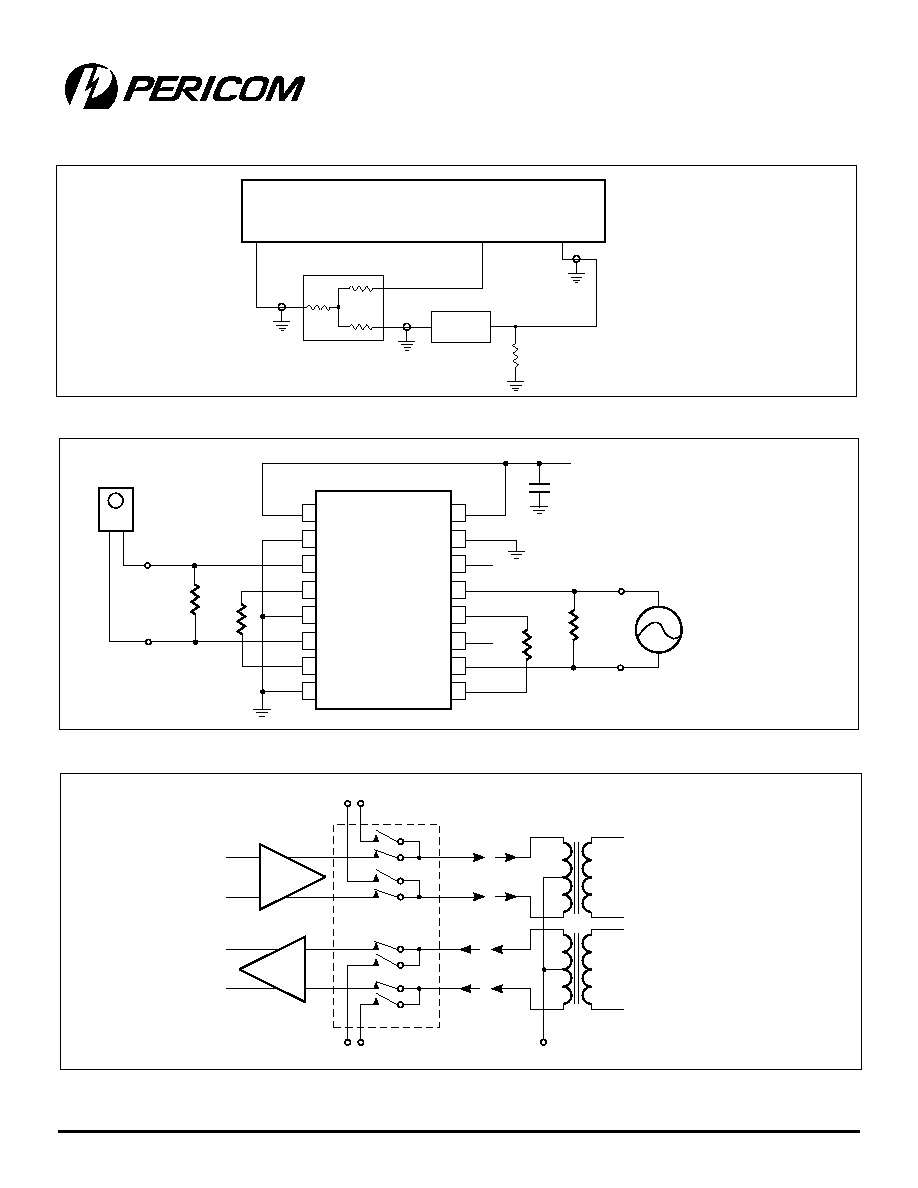
Figure 1. Switching Time
Test Circuits
3V
EN
S
D
GND
PI3L100
75
3.3V
Vcc
35 pF
V
OUT
I
N
DIGITAL
INPUT
ANALOG
OUTPUT
t
ON
t
OFF
50%
90%
50%
90%
t
r
a
P
e
g
a
k
c
a
P
n
i
P
e
r
u
t
a
r
e
p
m
e
T
Q
0
0
1
L
3
I
P
)
Q
(
P
O
S
Q
6
1
C
∞
5
8
+
o
t
C
∞
0
4
≠
L
0
0
1
L
3
I
P
)
L
(
P
O
S
S
T
6
1
C
∞
5
8
+
o
t
C
∞
0
4
≠
Ordering Information
5
PI3L100
3.3V, Wide Bandwidth Quad 2:1, Mux/Demux LanSwitch
12345678901234567890123456789012123456789012345678901234567890121234567890123456789012345678901212345678901234567890123456789012123456789012
12345678901234567890123456789012123456789012345678901234567890121234567890123456789012345678901212345678901234567890123456789012123456789012
PS8504 11/13/00
Figure 2. Gain/Phase Crosstalk, Off Isolation
S1
R1
T1
HP4195A
HP11667A
100
PI3L100
Figure 3. Differential Crosstalk Measurement
1
2
3
4
5
6
7
8
S
IA0
IA1
YA
IB0
IB1
YB
GND
16
15
14
13
12
11
10
9
V
CC
Z
ID0
ID1
YD
IC0
IC1
YC
100
100
Vo
DSO
V
CC
= 3.3V
0.1
µ
F
100
100
PULSE
GENERATOR
PI3L100
Figure 4a. Full Duplex Transceiver
TX1
PI3L100
TRANSMIT 2
RX1
RECEIVE 2
OFFSET ADJUST