
1
PS8754A 11/02/04
Pin Description
Pin Name
Description
I
A
N
to
I
D
N
Data Inputs
S
Select Inputs
EN
Enable
Y
A
to Y
D
Data Outputs
GND
Ground
V
CC
Power
Truth Table
(1)
EN
S
Y
A
Y
B
Y
C
Y
D
Function
H
X
Hi-Z
Hi-Z
Hi-Z
Hi-Z
Disable
L
L
IA0
IB0
IC0
ID0
S=0
L
H
IA1
IB1
IC1
ID1
S=1
Features
� Near-Zero propagation delay
� 5 switches connect inputs to outputs
� High signal passing bandwidth (500MHz)
� Beyond Rail-to-Rail switching
� 5V I/O tolerant with 3.3V supply
� 2.5V and 3.3V supply voltage operation
� Hot insertion capable
� Industrial operating temperature: -40�C to +85�C
� 2KV ESD Protection (human body model)
� Latch-up performance >250mA per JESD17
� Packaging (Pb-free & Green available):
� 16-pin QSOP (Q)
� 16-pin TSSOP (L)
� 20-contact TQFN (ZH)
Low On-Resistance, 3.3V High-Bandwidth
4-Port, 2:1 Mux/DeMux VideoSwitch
Notes:
1. H=High Voltage Level
L=Low Voltage Level
Description
Pericom Semiconductor's PI3V312 is a 4-port, 2:1 Multiplexer/
Demultiplexer with 3-state outputs. The switch introduces no ad-
ditional ground bounce noise or propagation delay.
Low On-Resistance and High bandwidth make it ideal for video
and other applications. Also this device has exceptionally low
crosstalk and off-isolation, which is far greater than most analog
switches offered today. A single 3.3V supply is all that is required
for operation.
The PI3V312 offers a high-performance (500MHz), low-cost solu-
tion to switch between video signals that have high bandwidth.
PI3V312
Pin Configuration
Block Diagram
EN
V
CC
S
1
I
A
0
2
I
D
0
I
A
1
3
I
D
1
Y
A
4
Y
D
I
B
0
5
16
I
C
0
I
B
1
6
15
I
C
1
Y
B
7
14
Y
C
8
13
12
GND
11
10
9
16-pin
L, Q
20-Contact
ZH
N.C.
EN
I
D
0
I
D
1
Y
D
I
C
0
I
C
1
Y
C
S
I
A
0
IA
1
Y
A
I
B
0
I
B
1
Y
B
N.C.
GND
N.C.
N.C.
V
CC
19
18
17
16
15
14
13
12
1
20
10
11
2
3
4
5
6
7
8
9
I
A
0
EN
S
I
A
1
I
B
0
I
B
1
I
C
0
I
C
1
Y
A
Y
B
Y
C
Y
D
I
D
0 I
D
1
2
PS8754A 11/02/04
PI3V312
Low On-Resistance, 3.3V High-Bandwidth
4-Port, 2:1 Mux/DeMux VideoSwitch
Storage Temperature ................................................ �65�C to +150�C
Ambient Temperature with Power Applied ............... �40�C to +85�C
Supply Voltage to Ground Potential ........................... �0.5V to +4.6V
DC Input Voltage ........................................................ �0.5V to +6.0V
DC Output Current................................................................... 120mA
Power Dissipation ....................................................................... 0.5W
Note:
Stresses greater than those listed under MAXIMUM
RATINGS may cause permanent damage to the device. This is a
stress rating only and functional operation of the device at these
or any other conditions above those indicated in the operational
sections of this specification is not implied. Exposure to absolute
maximum rating conditions for extended periods may affect re-
liability.
Maximum Ratings
(Above which the useful life may be impaired. For user guidelines, not tested.)
DC Electrical Characteristics, 3.3V Supply
(Over Operating Range, T
A
= �40�C to +85�C, V
CC
= 3.3V � 10%)
Parameters
Description
Test Conditions
(1)
Min.
Typ
(2)
Max. Units
V
IH
Input HIGH Voltage
Guaranteed Logic HIGH Level
2.0
V
V
IL
Input LOW Voltage
Guaranteed Logic LOW Level
�0.5
0.8
V
IK
Clamp Diode Voltage
V
CC
= Min., I
IN
= �18 mA
-1.3
�1.8
I
IH
Input HIGH Current
V
CC
= Max., V
IN
= V
CC
�1
�A
I
IL
Input LOW Current
V
CC
= Max., V
IN
= GND
�1
I
OZH
High Impedance Output Current 0 Y, I
N
V
CC
�1
R
ON
Switch On-Resistance
(4)
V
CC
= Min., V
IN
= 0V,
I
ON
= 48 mA or -64mA
4
6
V
CC
= Min., V
IN
= 3.6V, I
ON
= -15 mA
5
8
DC Electrical Characteristics, 2.5V Supply
(Over Operating Range, T
A
= �40�C to +85�C, V
CC
= 2.5V � 10%)
Parameters
(5)
Description
Test Conditions
Min.
Typ.
Max.
Units
V
IH
Input HIGH Voltage
Guaranteed Logic HIGH Level
1.8
�
V
CC
+ 0.3
V
V
IL
Inout LOW Voltage
Guaranteed Logic LOW Level
�0.3
�
0.8
V
IK
Clamp Diode Voltage
V
CC
= Max., I
IN
= �6mA
�
�0.7
�1.8
I
IH
Input HIGH Current
V
CC
= Max., V
IN
= V
CC
�
�
�1
�A
I
IL
Input LOW Current
V
CC
= Max., V
IN
= GND
�
�
�1
I
OZH
High Impedance Current
(3)
0 Y, In V
CC
�
�
�1
R
ON
Switch On-Resistance
(4)
V
CC
= Min., V
IN
= 0V,
I
ON
= �48mA
�
6
8
V
CC
= Min., V
IN
= 2.25V,
I
ON
= -15mA
�
7
14
3
PS8754A 11/02/04
PI3V312
Low On-Resistance, 3.3V High-Bandwidth
4-Port, 2:1 Mux/DeMux VideoSwitch
Notes:
1. For Max. or Min. conditions, use appropriate value specified under Electrical Characteristics for the applicable device.
2. Typical values are at V
CC
= 3.3V, +25�C ambient.
Notes:
1. For Max. or Min. conditions, use appropriate value specified under Electrical Characteristics for the applicable device type.
2. Typical values are at V
CC
= 3.3V, T
A
= 25�C ambient and maximum loading.
3. Not more than one output should be shorted at one time. Duration of the test should not exceed one second.
4. Measured by the voltage drop between Y and In pin at indicated current through the switch. On-Resistance is determined by the lower of the
voltages on the two (Y, In) pins.
5. This parameter is determined by device characterization but is not production tested.
Power Supply Characteristics
Parameters
Description
Test Conditions
(1)
Min. Typ.
(2)
Max.
Units
I
CC
Quiescent Power Supply Current
V
CC
= 3.6V, V
IN
= GND or V
CC
0.8
mA
Capacitance
(T
A
= 25�C f = 1 MHz)
Parameters
(5)
Description
Test Conditions
Typ.
Units
C
IN
Input Capacitance
V
IN
= 0V
3.0
pF
C
OFF(IN)
In Capacitance, Switch Off
3.5
C
OFF(Y)
Y Capacitance, Switch Off
7.0
C
ON
Y/In Capacitance, Switch On
10.0
Dynamic Electrical Characteristics Over the Operating Range
(T
A
= -40� to +85�, V
CC
= 3.3V � 10%)
Parameter
Description
Test Condition
Min.
Typ.
Max.
Units
X
TALK
Crosstalk
See Test Diagram (f = 100MHz)
-60
dB
O
IRR
Off-Isolation
See Test Diagram (f = 100MHz)
-60
BW
-3dB Bandwidth
See Test Diagram; C
L
= 0pF
100
500
MHz
4
PS8754A 11/02/04
PI3V312
Low On-Resistance, 3.3V High-Bandwidth
4-Port, 2:1 Mux/DeMux VideoSwitch
Switching Characteristics over 2.5V Operating Range
Parameters
Description
Conditions
(1)
Com.
Units
Min.
Max.
t
PLH
t
PHL
Propagation Delay
(2,3)
Y to In, In to Y
See Test Diagram
0.3
ns
t
PZH
t
PZL
Enable Time S or EN to Y or In
See Test Diagram
1.5
15.0
t
PHZ
t
PLZ
Disable Time S or EN to Y or In
1.5
12.0
Switching Characteristics over 3.3V Operating Range
Parameters
Description
Conditions
(1)
Com.
Units
Min.
Typ.
Max.
t
PLH
t
PHL
Propagation Delay
(2,3)
Y to In, In to Y
See Test Diagram
0.3
ns
t
PZH
t
PZL
Enable Time S or EN to Y or In
See Test Diagram
1.5
9.0
t
PHZ
t
PLZ
Disable Time S or EN to Y or In
1.5
9.0
Notes:
1. See test circuit and waveforms.
2. This parameter is guaranteed but not tested on Propagation Delays.
3. The switch contributes no propagational delay other than the RC delay of the On-Resistance of the switch and the load capacitance. The time
constant for the switch alone is of the order of 0.30ns for 10pF load. Since this time constant is much smaller than the rise/fall times of typical
driving signals, it adds very little propagational delay to the system. Propagational delay of the switch when used in a system is determined by
the driving circuit on the driving side of the switch and its interaction with the load on the driven side.
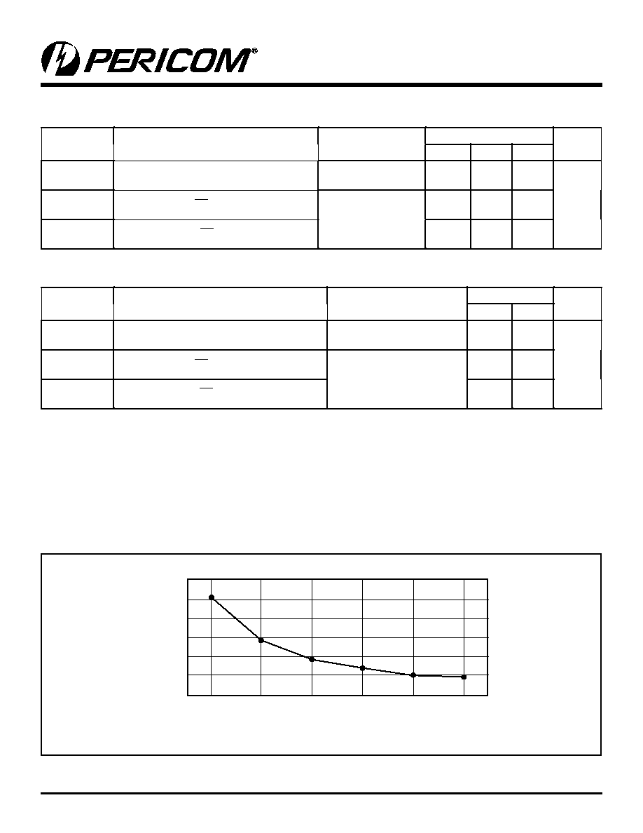
Bandwidth vs Capacitance
3db Bandwidth
600
500
400
300
200
100
0
0 pf
10 pf
20 pf
30 pf
40 pf
50 pf
Capacitance Load
5
PS8754A 11/02/04
PI3V312
Low On-Resistance, 3.3V High-Bandwidth
4-Port, 2:1 Mux/DeMux VideoSwitch
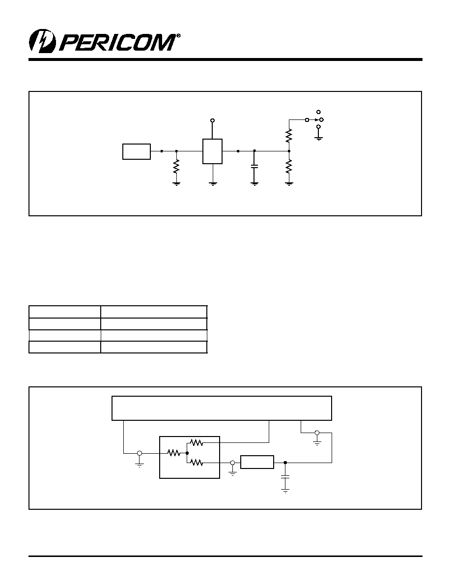
Test Circuit for Electrical Characteristics
(1)
Notes:
1. C
L
= Load capacitance: includes jig and probe capacitance.
2. R
T
= Termination resistance: should be equal to Z
OUT
of the Pulse Generator
3. Waveform 1 is for an output with internal conditions such that the output is low except when disabled by the output control.
Waveform 2 is for an output with internal conditions such that the output is high except when disabled by the output control.
4. All input impulses are supplied by generators having the following characteristics: PRR MHz, Z
O
= 50, t
R
2.5ns, t
F
2.5ns.
5. The outputs are measured one at a time with one transition per measurement.
Test Circuit for Dynamic Electrical Characteristics
Switch Positions
Test
Switch
t
PLZ
, t
PZL
6.0V
t
PHZ
, t
PZH
GND
Prop Delay
Open
R
T
10pF
C
L
V
CC
V
IN
V
OUT
200-ohm
200-ohm
6.0V
Pulse
Generator
D.U.T
V
CC
D.U.T
T1
R1
S1
HP11667A
C
L
HP4396