
1
PS8530B 08/13/04
Truth Table
(1)
Function
BE
A0-7
Disconnect
H
Hi-Z
Connect
L
B0-7
Description
Pericom Semiconductor's PI3VT series of logic circuits are produced
using the Company's advanced submicron CMOS technology,
achieving industry leading performance.
The PI3VT3245 is a 2.5V or 3.3V 8-bit, 2-port bus switch
designed with a low On-Resistance (5). The switches are turned
ON or enabled by the Bus Enable (BE) input signal.
Given a 3.3V supply and an input voltage of 3.3V, the switch
translates to an output voltage of 2.5V. Similarly, when operated
with a 2.5V supply and given 2.5V inputs, the device translates
the outputs to 1.8V.
Notes:
1. H = High Voltage Level
L = Low Voltage Level
Hi-Z = High Impedance
Block Diagram
Pin Description
Pin Name
Description
BE
Bus Enable Input (Active Low)
A
0
-A
7
Bus A
B
0
-B
7
Bus B
V
CC
Power
GND
Ground
Pin Configuration
Features
∑ Near-Zero propagation delay
∑ Low On-Resistance switches connect inputs to outputs
∑ 2.5V to 3.3V Supply voltage operation
∑ 2.5V or 1.8V switching
∑ Packaging (Pb-free & Green available):
≠ 20-pin, 150-mil wide plastic QSOP (Q)
≠ 20-pin, 173-mil wide plastic TSSOP (L)
Applications
∑ 3.3V to 2.5V level shifting (voltage translation)
∑ 2.5V to 1.8V level shifting (voltage translation)
PI3VT3245
8-Bit, 2-Port, Low Voltage
Translator Bus Switch
V
CC
BE
B
0
B
1
B
2
B
3
B
4
B
5
B
6
B
7
20
19
18
17
16
15
14
13
12
11
1
2
3
4
5
6
7
8
9
10
NC
A
0
A
1
A
2
A
3
A
4
A
5
A
6
A
7
GND
BE
A
7
A
0
B
7
B
0

2
PS8530B 08/13/04
PI3VT3245
8-Bit, 2-Port, Low Voltage
Translator Bus Switch
Storage Temperature ......................................................... ≠65∞C to +150∞C
Ambient Temperature with Power Applied ........................ ≠40∞C to +85∞C
Supply Voltage to Ground Potential..................................... ≠0.5V to +4.6V
DC Input Voltage ................................................................. ≠0.5V to +5.5V
DC Output Current............................................................................ 120mA
Power Dissipation ................................................................................ 0.5W
Note:
Stresses greater than those listed under MAXIMUM RATINGS
may cause permanent damage to the device. This is a stress
rating only and functional operation of the device at these or any
other conditions above those indicated in the operational sec-
tions of this specification is not implied. Exposure to absolute
maximum rating conditions for extended periods may affect
reliability.
Maximum Ratings
(Above which the useful life may be impaired. For user guidelines, not tested.)
Notes:
1. For Max. or Min. conditions, use appropriate value specified under Electrical Characteristics for the applicable device type.
2. Typical values are at V
CC
= 3.3V, T
A
= 25∞C ambient and maximum loading.
3. Not more than one output should be shorted at one time. Duration of the test should not exceed one second.
4. Measured by the voltage drop between A and B pin at indicated current through the switch. On-Resistance is determined
by the lower of the voltages on the two (A,B) pins.
5. This parameter is determined by device characterization but is not production tested.
Capacitance
(T
A
= 25∞C, f = 1 MHz)
Parameters
(5)
Description
Test Conditions
Typ.
Units
C
IN
Input Capacitance
V
IN
= 0V
3.5
pF
C
OFF
A/B Capacitance, Switch Off
5.0
C
ON
A/B Capacitance, Switch On
11.2
DC Electrical Characteristics
(Over Operating Range, T
A
= ≠40∞C to +85∞C, V
CC
= 3.3V ±10%)
Parameters
Description
Test Conditions
(1)
Min.
Typ.
(2)
Max.
Units
V
IH
Input HIGH Voltage
Guaranteed logic HIGH level
2.0
V
CC
+0.3V
V
V
IL
Input LOW Voltage
Guaranteed logic LOW level
-0.5
0.8
I
IH
Input HIGH Current
V
CC
= Max., V
IN
= V
CC
±1
µA
I
IL
Input LOW Current
V
CC
= Max., V
IN
= GND
±1
I
OZH
High Impedance Output
Current
0 A, B V
CC
±1
R
ON
Switch On-Resistance
V
CC
= Min, V
IN
= 0V, I
ON
= -8mA
5
8
V
CC
= Min., V
IN
= 1.7V, I
ON
= -8mA
15
22
V
CC
= 2.3V., V
IN
= 0V, I
ON
= -8mA
6
9
V
CC
= 2.3V., V
IN
= 1.3V, I
ON
= -8mA
25
30
Vp
Pass Voltage
V
IN
= V
CC
= 3.3V, I
OUT
= -5µA
2.3
2.5
2.9
V
V
IN
= V
CC
= 2.5V, I
OUT
= -5µA
1.8

3
PS8530B 08/13/04
PI3VT3245
8-Bit, 2-Port, Low Voltage
Translator Bus Switch
Power Supply Characteristics
Parameters
Description
Test Conditions
(1)
Min.
Typ.
(2)
Max.
Units
I
CC
Quiescent Power Supply Current
V
CC
= Max.
V
IN
= GND or V
CC
3
µA
I
CC
Quiescent Current per Input HIGH
V
IN
= 3V
(3)
50
Notes:
1. For Max. or Min. conditions, use appropriate value specified under Electrical Characteristics for the applicable device.
2. Typical values are at V
CC
= 3.3V, +25∞C ambient.
3. Per driven input (control input only); A and B pins do not contribute to I
CC
.
Notes:
1. See test circuit and waveforms.
2. This parameter is guaranteed but not tested on Propagation Delays.
3. The bus switch contributes no propagational delay other than the RC delay of the On-Resistance of the switch and the load capacitance. The
time constant for the switch alone is of the order of 0.25ns for 50pF load. Since this time constant is much smaller than the rise/fall times of
typical driving signals, it adds very little propagational delay to the system. Propagational delay of the bus switch when used in a system is
determined by the driving circuit on the driving side of the switch and its interaction with the load on the driven side.
Switching Characteristics over 2.5V ±0.2V Operating Range
Parameters
Description
Conditions
(1)
Com.
Units
Min.
Max.
t
PLH
t
PHL
Propogation Delay
(2,3)
Ax to Bx
C
L
= 50pF,
R
L
= 500
0.25
ns
t
PZH
t
PZL
Enable Time BE to Ax or Bx
C
L
= 50pF,
R
L
= 500,
R = 500
1.5
9.8
t
PHZ
t
PLZ
Disable Time BE to Ax or Bx
1.5
8.3
Switching Characteristics over 3.3V ±0.3V Operating Range
Parameters
Description
Conditions
(1)
Com.
Units
Min.
Max.
t
PLH
t
PHL
Propogation Delay
(2,3)
Ax to Bx
C
L
= 50pF,
R
L
= 500
0.25
ns
t
PZH
t
PZL
Enable Time BE to Ax or Bx
C
L
= 50pF,
R
L
= 500,
R = 500
1.5
9.8
t
PHZ
t
PLZ
Disable Time BE to Ax or Bx
1.5
8.3
4
PS8530B 08/13/04
PI3VT3245
8-Bit, 2-Port, Low Voltage
Translator Bus Switch
.252
.260
.047
1.20
.002
.006
SEATING
PLANE
.0256
BSC
.018
.030
.004
.008
.238
.269
1
20
.169
.177
X.XX
X.XX
DENOTES CONTROLLING
DIMENSIONS IN MILLIMETERS
0.05
0.15
6.1
6.7
0.45
0.75
0.09
0.20
4.3
4.5
6.4
6.6
0.65
0.19
0.30
.007
.012
Max
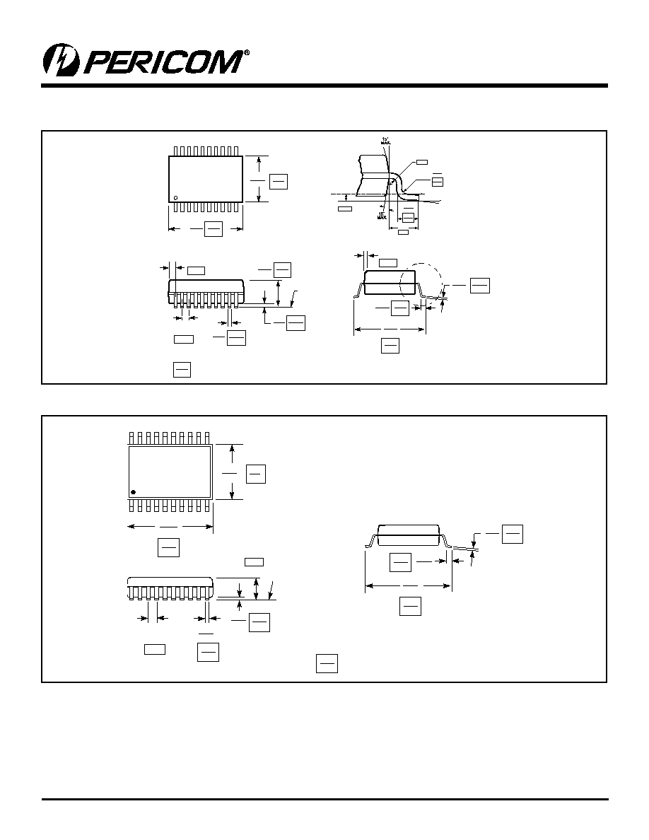
Packaging Mechanical: 20-pin QSOP (Q)
.337
.344
.053
.069
.004
.010
SEATING
PLANE
.025
BSC
.007
.010
.228
.244
.150
.157
1
20
.016
.050
X.XX
X.XX
DENOTES DIMENSIONS
IN MILLIMETERS
0.635
8.56
8.74
1.35
1.75
5.79
6.19
0.41
1.27
0.101
0.254
.008
.012
0.203
0.305
3.81
3.99
0.178
0.254
.058
1.47
.015 x 45∞
0.38
REF
Detail A
Detail A
.008
0.20
MIN.
Guage Plane
.010
0.254
.041
1.04
REF
.016
.035
0.41
0.89
0∞-6∞
.008
.013
0.20
0.33
Packaging Mechanical: 20-pin TSSOP (L)

5
PS8530B 08/13/04
PI3VT3245
8-Bit, 2-Port, Low Voltage
Translator Bus Switch
Ordering Information
Ordering Code
Packaging Code
Package Description
PI3VT3245L
L
20-pin TSSOP
PI3VT3245LE
L
Pb-free & Green, 20-pin TSSOP
PI3VT3245Q
Q
20-pin QSOP
PI3VT3245QE
Q
Pb-free & Green, 20-pin QSOP
Notes:
1. Thermal characteristics can be found on the company web site at www.pericom.com/packaging/
Pericom Semiconductor Corporation ∑ 1-800-435-2336 ∑ www.pericom.com