
1
PS7006C 06/27/01
PI49FCT805T/2805T Logic Block Diagram
PI49FCT806T Logic Block Diagram
Product Description
Pericom Semiconductors PI49FCT series of logic circuits are
produced using the Companys advanced 0.8 micron CMOS
technology, achieving industry leading speed grades.
The PI49FCT805T and PI49FCT2805T are non-inverting clock
drivers. The PI49FCT806T is an inverting clock driver designed with
two independent groups of buffers that have Hi-Z state Output
Enable inputs (active LOW) with a 1-in, 5-out configuration per
group. Each clock driver consists of two banks of drivers, driving
five outputs each from a standard TTL-compatible CMOS input.
The PI49FCT2805T also features a 25-ohm on-chip resistor for lower
noise.
Product Features
Extremely low output skew: 0.5ns
Monitor output pin
Clock busing with Hi-Z state control
TTL input and CMOS output compatible
Extremely low static power (1mW, typ.)
Hysteresis on all inputs
Packages available:
20-pin 209 mil wide SSOP (H)
20-pin 300 mil wide SOIC (S)
20-pin 150 mil wide QSOP (Q)
Device models available on request
Industrial Operation at -40∫C to +85∫C
OE
B
IN
A
OA
0≠4
IN
B
OE
A
OB
0≠4
MON
5
5
OE
B
IN
A
OA
0≠4
IN
B
OE
A
OB
0≠4
MON
5
5
Fast CMOS
Buffer/Clock Driver
12345678901234567890123456789012123456789012345678901234567890121234567890123456789012345678901212345678901234567890123456789012123456789012
12345678901234567890123456789012123456789012345678901234567890121234567890123456789012345678901212345678901234567890123456789012123456789012
PI49FCT805T
PI49FCT2805T
PI49FCT806T

2
PS7006C 06/27/01
12345678901234567890123456789012123456789012345678901234567890121234567890123456789012345678901212345678901234567890123456789012123456789012
12345678901234567890123456789012123456789012345678901234567890121234567890123456789012345678901212345678901234567890123456789012123456789012
PI49FCT805T
PI49FCT2805T/PI49FCT806T
Fast CMOS Buffer/Clock Driver
PI49FCT805T/2805T Product Pin Configuration
Inputs
Outputs
OE
A
, OE
B
IN
A
, IN
B
OA
N
, OB
N
MON
L
L
L
L
L
H
H
H
H
L
Z
L
H
H
Z
H
PI49FCT805T/2805T Truth Table
(1)
Note:
1. H= High Voltage Level
L= Low Voltage Level
Z= High Impedance
Inputs
Outputs
OE
A
, OE
B
IN
A
, IN
B
OA
N
, OB
N
MON
L
L
H
H
L
H
L
L
H
L
Z
H
H
H
Z
L
PI49FCT806T Truth Table
(1)
PI49FCT806T Product Pin Configuration
1
2
3
4
5
6
7
8
9
10
20
19
18
17
16
15
14
13
12
11
Vcc
A
OA
0
OA
1
OA
2
GND
A
OA
3
OA
4
GND
B
OE
A
IN
A
Vcc
B
OB
0
OB
1
OB
2
GND
B
OB
3
OB
4
MON
OE
B
IN
B
1
2
3
4
5
6
7
8
9
10
20
19
18
17
16
15
14
13
12
11
Vcc
A
OA
0
OA
1
OA
2
GND
A
OA
3
OA
4
GND
B
OE
A
IN
A
Vcc
B
OB
0
OB
1
OB
2
GND
B
OB
3
OB
4
MON
OE
B
IN
B
Product Pin Description
e
m
a
N
n
i
P
n
o
it
p
i
r
c
s
e
D
E
O
A
E
O
,
B
)
W
O
L
e
v
it
c
A
(
st
u
p
n
I
el
b
a
n
E
t
u
p
t
u
O
e
t
a
t
S
Z
-i
H
N
I
A
N
I
,
B
st
u
p
n
I
k
c
o
l
C
A
O
N
B
O
,
N
)
T
5
0
8
2
T
C
F
9
4
I
P
/
T
5
0
8
T
C
F
9
4
I
P
(
st
u
p
t
u
O
k
c
o
l
C
A
O
N
B
O
,
N
)
T
6
0
8
T
C
F
9
4
I
P
(
t
u
p
t
u
O
k
c
o
l
C
N
O
M
t
u
p
t
u
O
r
o
ti
n
o
M
D
N
G
d
n
u
o
r
G
V
C
C
r
e
w
o
P
20-Pin
H, Q, S
20-Pin
H, Q, S

3
PS7006C 06/27/01
12345678901234567890123456789012123456789012345678901234567890121234567890123456789012345678901212345678901234567890123456789012123456789012
12345678901234567890123456789012123456789012345678901234567890121234567890123456789012345678901212345678901234567890123456789012123456789012
PI49FCT805T
PI49FCT2805T/PI49FCT806T
Fast CMOS Buffer/Clock Driver
DC Electrical Characteristics
(Over the Operating Range, T
A
= 40∞C to +85∞C, V
CC
= 5.0V ± 5%)
Parameters Description
Test Conditions
(1)
Min.
Typ
(2)
Max.
Units
V
OH
Output HIGH Voltage
V
CC
= Min., V
IN
= V
IH
or V
IL
I
OH
= 24.0mA
2.4
3.3
V
V
OL
Output LOW Current
V
CC
= Min., V
IN
= V
IH
or V
IL
I
OL
= 64mA
0.3
0.55
V
I
OL
= 12mA (25
)
0.3
0.50
V
V
IH
Input HIGH Voltage
Guaranteed Logic HIGH Level
2.0
V
V
IL
Input LOW Voltage
Guaranteed Logic LOW Level
0.8
V
I
IH
Input HIGH Current
V
CC
= Max.
V
IN
= V
CC
1
µA
I
IL
Input LOW Current
V
CC
= Max.
V
IN
= GND
1
µA
I
OZH
High Impedance
V
CC
= Max.
V
OUT
= V
CC
1
µA
I
OZL
Output Current
V
OUT
= GND
1
µA
I
I
Input HIGH Current
V
CC
= Max., V
IN
=V
CC
(Max.)
20
µA
V
IK
Clamp Diode Voltage
V
CC
= Min., I
IN
= 18mA
0.7
1.2
V
I
OS
Short Circuit Current
V
CC
= Max.
(3)
, V
OUT
= GND
60
120
225
mA
V
H
Input Hysteresis
V
CC
= 5 V
200
mV
Storage Temperature ............................................................. 65∞C to +150∞C
Ambient Temperature with Power Applied .............................. -40∞C to +85∞C
Supply Voltage to Ground Potential (Inputs & Vcc Only) ....... 0.5V to +7.0V
Supply Voltage to Ground Potential (Outputs & D/O Only) .... 0.5V to +7.0V
DC Input Voltage ..................................................................... 0.5V to +7.0V
DC Output Current ............................................................................... 120mA
Power Dissipation ................................................................................... 0.5W
Note:
Stresses greater than those listed under MAXIMUM
RATINGS may cause permanent damage to the de-
vice. This is a stress rating only and functional opera-
tion of the device at these or any other conditions
above those indicated in the operational sections of
this specification is not implied. Exposure to absolute
maximum rating conditions for extended periods may
affect reliability.
Capacitance
(T
A
= 25∞C, f = 1 MHz)
Parameters
(4)
Description
Test Conditions
Typ
Max.
Units
C
IN
Input Capacitance
V
IN
= 0 V
6
10
pF
C
OUT
Output Capacitance
V
OUT
= 0 V
8
12
pF
Notes:
1. For Max. or Min. conditions, use appropriate value specified under Electrical Characteristics for the applicable device type.
2. Typical values are at V
CC
= 5.0V, +25∞C ambient and maximum loading.
3. Not more than one output should be shorted at one time. Duration of the test should not exceed one second.
4. This parameter is determined by device characterization but is not production tested.
Maximum Ratings
(Above which the useful life may be impaired. For user guidelines, not tested.)

4
PS7006C 06/27/01
12345678901234567890123456789012123456789012345678901234567890121234567890123456789012345678901212345678901234567890123456789012123456789012
12345678901234567890123456789012123456789012345678901234567890121234567890123456789012345678901212345678901234567890123456789012123456789012
PI49FCT805T
PI49FCT2805T/PI49FCT806T
Fast CMOS Buffer/Clock Driver
Power Supply Characteristics
Parameters Description
Test Conditions
(1)
Min.
Typ
(2)
Max.
Units
I
CC
Quiescent Power
V
CC
= Max.
V
IN
= GND or V
CC
3
30
µA
Supply Current
I
CC
Supply Current per
V
CC
= Max.
V
IN
= 3.4V
(3)
0.5
2.0
mA
Input @ TTL HIGH
I
CCD
Supply Current per
V
CC
= Max.,
V
IN
= V
CC
0.15
0.25
mA/
Input per MHz
(4)
Outputs Open
V
IN
= GND
MHz
OE
A
= OE
B
= GND
Per Output Toggling
50% Duty Cycle
I
C
Total Power Supply
V
CC
= Max.,
V
IN
= V
CC
7.7
14.0
(5)
mA
Current
(6)
Outputs Open
V
IN
= GND
f
I
= 10 MH
Z
50% Duty Cycle
V
IN
= 3.4V
8.0
15.0
(5)
OE
A
= OE
B
= GND
V
IN
= GND
Five Outputs Toggling
V
CC
= Max.,
V
IN
= V
CC
4.3
8.4
(5)
Outputs Open
V
IN
= GND
f
I
= 2.5 MH
Z
50% Duty Cycle
OE
A
= OE
B
= GND
V
IN
= 3.4V
4.8
10.4
(5)
Eleven Outputs
V
IN
= GND
Toggling
Notes:
1. For Max. or Min. conditions, use appropriate value specified under Electrical Characteristics for the applicable device.
2. Typical values are at Vcc = 5.0V, +25∞C ambient.
3. Per TTL driven input (V
IN
= 3.4V); all other inputs at Vcc or GND.
4. This parameter is not directly testable, but is derived for use in Total Power Supply Calculations.
5. Values for these conditions are examples of the Icc formula. These limits are guaranteed but not tested.
6. I
C
=I
QUIESCENT
+ I
INPUTS
+ I
DYNAMIC
I
C
= I
CC
+
I
CC
D
H
N
T
+ I
CCD
(f
CP
/2 + f
I
N
I
)
I
CC
= Quiescent Current
I
CC
= Power Supply Current for a TTL High Input (V
IN
= 3.4V)
D
H
= Duty Cycle for TTL Inputs High
N
T
= Number of TTL Inputs at D
H
I
CCD
= Dynamic Current Caused by an Input Transition Pair (HLH or LHL)
f
CP
= Clock Frequency for Register Devices (Zero for Non-Register Devices)
f
I
= Input Frequency
N
I
= Number of Inputs at f
I
All currents are in milliamps and all frequencies are in megahertz.
5
PS7006C 06/27/01
12345678901234567890123456789012123456789012345678901234567890121234567890123456789012345678901212345678901234567890123456789012123456789012
12345678901234567890123456789012123456789012345678901234567890121234567890123456789012345678901212345678901234567890123456789012123456789012
PI49FCT805T
PI49FCT2805T/PI49FCT806T
Fast CMOS Buffer/Clock Driver
PI49FCT805/806T Switching Characteristics over Operating Range
Notes:
1. See test circuit and wave forms.
2. Minimum limits are guaranteed but not tested on Propagation Delays.
3. Skew measured at worse cast temperature (max. temp).
4. This parameter is guaranteed but not production tested.
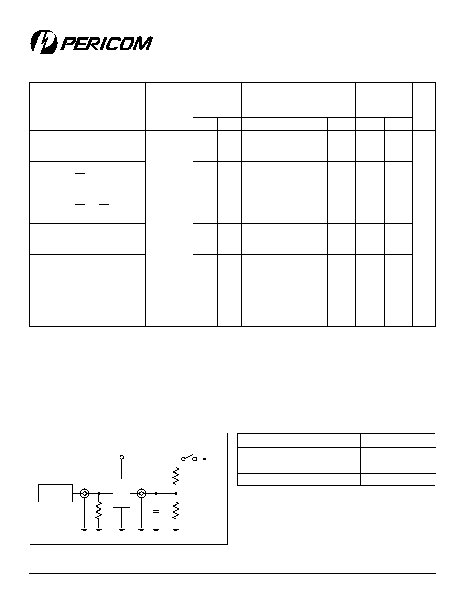
Tests Circuits For All Outputs
(1)
Pulse
Generator
D.U.T.
V
IN
R
T
V
OUT
C
L
500
500
50pF
V
CC
7.0V
s
r
e
t
e
m
a
r
a
P
n
o
it
p
i
r
c
s
e
D
s
n
o
it
i
d
n
o
C
)
1
(
/
T
5
0
8
2
/
T
5
0
8
T
6
0
8
/
T
A
5
0
8
2
/
T
A
5
0
8
T
A
6
0
8
/
T
B
5
0
8
2
/
T
B
5
0
8
T
B
6
0
8
/
T
C
5
0
8
2
/
T
C
5
0
8
T
C
6
0
8
s
ti
n
U
.
m
o
C
m
o
C
.
m
o
C
m
o
C
.
n
i
M
.
x
a
M
.
n
i
M
.
x
a
M
.
n
i
M
.
x
a
M
.
n
i
M
.
x
a
M
t
H
L
P
t
L
H
P
y
al
e
D
n
o
it
a
g
a
p
o
r
P
N
I
A
o
t
A
O
N
,
N
I
B
o
t
B
O
N
F
p
0
5
=
L
C
0
0
5
=
L
R
5
.
1
5
.
6
5
.
1
8
.
5
5
.
1
0
.
5
5
.
1
5
.
4
s
n
t
H
Z
P
t
L
Z
P
e
m
i
T
el
b
a
n
E
t
u
p
t
u
O
E
O
A
o
t
A
O
N
,
E
O
B
o
t
B
O
N
5
.
1
0
.
8
5
.
1
0
.
8
5
.
1
5
.
8
5
.
1
2
.
6
t
Z
H
P
t
Z
L
P
e
m
i
T
el
b
a
si
D
t
u
p
t
u
O
)
4
(
E
O
A
o
t
A
O
N
,
E
O
B
o
t
B
O
N
5
.
1
0
.
7
5
.
1
0
.
7
5
.
1
0
.
6
5
.
1
0
.
5
t
(
W
E
K
S
o) )
3
(
st
u
p
t
u
o
o
w
t
x
w
t
w
e
k
S
e
g
a
k
c
a
p
e
m
a
s
f
o
)
n
o
it
i
s
n
a
rt
e
m
a
s
(
7
.
0
5
.
0
4
.
0
4
.
0
t
(
W
E
K
S
p) )
3
(
e
ti
s
o
p
p
o
x
w
t
w
e
k
S
t(
s
n
o
it
i
s
n
a
rt
L
H
P
t
-
H
L
P
)
t
u
p
t
u
o
e
m
a
s
f
o
0
.
1
7
.
0
5
.
0
5
.
0
t
(
W
E
K
S
t) )
3
(
st
u
p
t
u
o
o
w
t
x
w
t
w
e
k
S
t
a
e
g
a
k
c
a
p
t
n
e
r
e
ff
i
d
f
o
e
r
u
t
a
r
e
p
m
e
t
e
m
a
s
)
n
o
it
i
s
n
a
rt
e
m
a
s
(
5
.
1
0
.
1
0
.
1
0
.
1
Test
Switch
Open Drain
Disable LOW
Closed
Enable LOW
All Other Inputs
Open
Definitions:
C
L
= Load capacitance: includes jig and probe capacitance.
R
T
= Termination resistance: should be equal to ZOUT of the
Pulse Generator.
Switch Position