1
PS8496A 09/08/04
3.3V 1:10 CMOS Clock Driver
Description
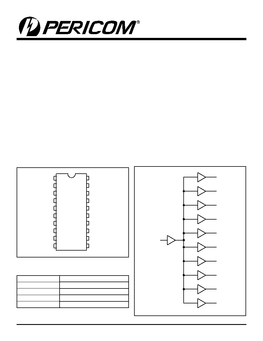
Pericom Semiconductor's PI49FCT32807 is a 3.3V very low-
skew clock buffer that produces ten outputs from a single low-
capacitance input. Excellent output signals to power and ground
ratio minimize power and ground noise, and also improves output
performance.
The PI49FCT32807 integrates series damping resistors on all
outputs.
Pin Configuration
Pin Description
Pin Name
Description
A
Input
B
0
-B
9
Outputs
GND
Ground
V
CC
Power
Block Diagram
PI49FCT32807
Features
∑ Low skew: < 200ps
∑ Fast switching frequency >133 MHz
∑ Fast output rise/fall time < 1.5ns
∑ Low propagation delay < 2.5ns
∑ Low input capacitance < 6.0pF
∑ 5V I/O Tolerant input
∑ Rail-to-Rail CMOS outputs
∑ Industrial Temperature: ≠40∞C to +85∞C
∑ 3.3V ±10% operation
∑ Packaging (Pb-free & Green Available):
≠ 20-pin 300-mil wide SOIC (S)
≠ 20-pin 150-mil wide QSOP (Q)
≠ 20-pin 209-mil wide SSOP (H)
VCC
A
1
20
B9
GND
2
19
B8
B0
3
18
GND
VCC
4
17
B7
B1
5
16
VCC
GND
6
15
B6
B2
7
14
GND
VCC
8
13
B5
B3
9
12
B4
GND
10
11
B0
A
B1
B2
B3
B4
B5
B6
B7
B8
B9

PI49FCT32807
3.3V 1:10 CMOS Clock Driver
2
PS8496A 09/08/04
Maximum Ratings
(Above which the useful life may be impaired. For user guidelines, not tested.)
Note:
Stresses greater than those listed under MAXIMUM
RATINGS may cause permanent damage to the
device. This is a stress rating only and functional operation
of the device at these or any other conditions above those
indicated in the operational sections of this specification is
not implied. Exposure to absolute maximum rating condi-
tions for extended periods may affect reliability.
DC Electrical Characteristics
(Over the Operating Range)
Symbol
Parameter
Test Condition
(1)
Min.
Typ.
Max.
Units
V
OH
Output High Voltage
V
CC
= 3V, V
IN
= V
IH
or V
IL
I
OH
= -8mA
2.4
3.0
V
V
OL
Output Low Voltage
V
CC
= 3V V
IH
or V
IL
I
OL
= 12mA
0.4
0.5
V
IH
Input High Voltage
Guaranteed Logic HIGH Level (Input pins)
2.0
505
V
IL
Input Low Voltage
Guaranteed Logic LOW Level (Input pins)
-0.5
0.8
I
IH
Input High Current
V
CC
= 3.6V
V
IN
= 3.6V
1
µA
I
IL
Input Low Current
V
CC
= 3.6V
V
IN
= 0V
-1
V
IK
Clamp Diode Voltage
V
CC
= Min., I
IN
= -18mA
-0.7
-1.2
V
I
OH
Output HIGH Current
V
CC
= 3.3V, V
IN
=V
IL
or V
IH,
V
OUT
= 1.5V
(5)
-25
-45
-80
mA
I
OL
Output LOW
Current
V
CC
= 3.3V, V
IN
=V
IL
or V
IH,
V
OUT
= 1.5V
(5)
25
45
90
I
OS
Short Circuit
(5)
Current
V
CC
= Max., V
OUT
= GND
(5)
-50
-100
-180
V
H
Input Hysteresis
150
mV
R
S
Internal Series Resistor
22
Storage Temperature ............................................................≠65∞C to +150∞C
Ambient Temperature with Power Applied ...........................≠40∞C to +85∞C
Supply Voltage to Ground Potential (Inputs & V
CC
Only).....≠0.5V to +7.0V
Supply Voltage to Ground Potential (Outputs & D/O Only) ..≠0.5V to +7.0V
DC Input Voltage ....................................................................≠0.5V to +7.0V
DC Output Current............................................................................... 120mA
Power Dissipation ................................................................................... 0.5W
Notes:
1. For Max. or Min. conditions, use appropriate value specified under Electrical Characteristics for the applicable device type.
2. Typical values are at V
CC
= 3.3V, +25∞C ambient and maximum loading.
3. V
OH
= V
CC
≠ 0.6V at rated current.
4. This parameter is determined by device characterization but is not production tested.
5. Not more than one output should be shorted at one time. Duration of the test should not exceed one second.

PI49FCT32807
3.3V 1:10 CMOS Clock Driver
3
PS8496A 09/08/04
Power Supply Characteristics
Parameters
Description
Test Conditions
(1)
Min.
Typ
(2)
Max.
Units
I
CC
Quiescent Power
Supply Current
V
CC
= Max.
V
IN
= GND
or V
CC
--
0.1
30
µA
I
CC
Supply Current per
Inputs @ TTL HIGH
V
CC
= Max.
V
IN
= V
CC
≠ 0.6V
(3)
--
47
300
I
CCD
Supply Current per
Input per MHz
(4)
V
CC
= Max.,
Outputs Open
Per Output Toggling
50% Duty Cycle
V
IN
= V
CC
V
IN
= GND
--
0.08
0.16
mA/
MHz
Notes:
1. For Max. or Min. conditions, use appropriate value specified under Electrical Characteristics for the applicable device.
2. Typical values are at V
CC
= 3.3V, +25∞C ambient.
3. Per TTL driven input (V
IN
= V
CC
≠ 0.6V); all other inputs at V
CC
or GND.
4. This parameter is not directly testable, but is derived for use in Total Power Supply Calculations.
5. Values for these conditions are examples of the I
C
formula. These limits are guaranteed but not tested.
Capacitance
(T
A
= 25∞C, f = 1 MHz)
Parameters
(1)
Description
Test Conditions
Typ
Max.
Units
C
IN
Input Capacitance
V
IN
= 0V
3.0
4
pF
C
OUT
Output Capacitance
V
OUT
= 0V
6
Notes:
1. This parameter is determined by device characterization but is not production tested.
Maximum Switching Characteristics
(Over operating range)
Symbol
Description
Condition
Max.
Units
(3)
t
PLH
t
PHL
Propagation Delay A to B
N
(3)
C
L
= 15pF
2.5
ns
t
R
/t
F
Rise/Fall Time
(2)
0.8V - 2.0V
1.5
t
SK(P)
Pulse Skew, same package
(1, 2)
C
L
= 15pF
0.35
t
SK(O)
Output Skew, same package
(1, 2)
0.20
t
SK(I)
Package Skew, different package
(1, 2)
0.55
F
IN
Input Frequency
(1, 2)
133
MHz
Notes:
1. Other loading condition is described on page 4, "Test Circuits for All Outputs."
2. These parameters are guaranteed by design.
3. Minimum propagation delay of 1.5ns is guaranteed by design.

PI49FCT32807
3.3V 1:10 CMOS Clock Driver
4
PS8496A 09/08/04
Tests Circuits for All Outputs
Switching Waveforms
Propagation Delay
Package Skew ≠ t
SK
(t)
Pulse Skew ≠ t
SK
(p)
Output Skew ≠ t
SK
(o)
Input
t
PLH
3V
1.5V
0V
Output
V
OH
1.5V
V
OL
t
PHL
2.0V
0.5V
t
R
t
F
Input
t
PLHx
3V
1.5V
0V
Ox
V
OH
1.5V
V
OL
t
PHLx
t
SK(o)
Oy
V
OH
1.5V
V
OL
t
SK(o)
t
PLHy
t
PHLy
t
SK(o)
= t
PLHy
≠ t
PLHx
or t
PHLy
≠ t
PHLx
Input
t
PLH
3V
1.5V
0V
Output
V
OH
1.5V
V
OL
t
PHL
t
SK(p)
= t
PHL
≠ t
PLH
Input
t
PLH1
3V
1.5V
0V
Package 1
Output
V
OH
1.5V
V
OL
t
PHL1
t
SK(t)
Package 2
Output
V
OH
1.5V
V
OL
t
SK(t)
t
PLH2
t
PHL2
t
SK(t)
= t
PLH2
≠ t
PLH1
or t
PHL2
≠ t
PHL1
Pulse
Generator
f = 125MHz
D.U.T.
50
C
L
15pF
V
CC

PI49FCT32807
3.3V 1:10 CMOS Clock Driver
5
PS8496A 09/08/04
SEATING
PLANE
.050
BSC
1
20
0-8∞
.2914
.2992
X.XX
X.XX
DENOTES CONTROLLING
DIMENSIONS IN MILLIMETERS
7.40
7.60
.496
.511
12.60
12.99
1.27
.0926
.1043
2.35
2.65
.394
.419
10.00
10.65
.0040
.0118
0.10
0.30
.013
.020
0.33
0.51
.010
.029
0.254
0.737
.0091
.0125
0.23
0.32
0.41
1.27
.016
.050
x 45∞
.020
.030
0.508
0.762
REF
.272
.295
.078
.002
SEATING
PLANE
.0098
Max.
.0256
BSC
.022
.037
.004
.009
.291
.322
1
20
.197
.220
0.25
X.XX
X.XX
DENOTES DIMENSIONS
IN MILLIMETERS
0.050
7.40
8.20
0.55
0.95
0.09
0.25
5.00
5.60
2.00
6.90
7.50
0.65
Max
Min
Packaging Mechanical: 20-pin SSOP (H)
Packaging Mechanical: 20-pin SOIC (S)