
1
PS7007B 01/13/99
3.3V Fast CMOS Buffer/Clock Driver
OA
0-4
5
OE
A
IN
A
OB
0-4
5
OE
B
IN
B
MON
PI49FCT3805 Logic Block Diagram
OA
0-4
5
OE
A
IN
A
OB
0-4
5
OE
B
IN
B
MON
PI49FCT3806 Logic Block Diagram
12345678901234567890123456789012123456789012345678901234567890121234567890123456789012345678901212345678901234567890123456789012123456789012
12345678901234567890123456789012123456789012345678901234567890121234567890123456789012345678901212345678901234567890123456789012123456789012
PI49FCT3805/PI49FCT3806
PI49FCT3805A/PI49FCT3806A
PI49FCT3805B/PI49FCT3806B
PI49FCT3805C/PI49FCT3806C
Product Description
Pericom Semiconductors PI49FCT series of logic circuits are
produced using the Companys advanced submicron CMOS
technology, achieving industry leading speed grades.
The PI49FCT3805 is a 3.3V non-inverting clock driver and the
PI49FCT3806 is a 3.3V inverting clock driver designed with two
independent groups of buffers. These buffers have 3-state Output
Enable inputs (active LOW) with a 1-in, 5-out configuration per
group. Each clock driver consist of two banks of drivers, driving five
outputs each from a standard TTL compatible CMOS input.
Features
3.3V version of PI49FCT805/806
Extremely low output skew: 0.5ns
Monitor ouput pin
Clock busing wih 3-state control
TTL inpu and CMOS output compatible
Industrial operation at40∞C to 85∞C
Extremely low static power (1mW, typ.)
Hysteresis on all inputs
Packages available:
20-pin 300-mil wide SOIC (S)
20-pin 150-mil wide QSOP (Q)
20-pin 209-mil wide SSOP (H)
Device models available on request

2
PS7007B 01/13/99
12345678901234567890123456789012123456789012345678901234567890121234567890123456789012345678901212345678901234567890123456789012123456789012
PI49FCT3805/3806
3.3V Fast CMOS Buffer/Clock Driver
Capacitance
(T
A
= 25∞C, f = 1 MHz)
Parameters
(1)
Description
Test Conditions
Typ
Max.
Units
C
IN
Input Capacitance
V
IN
= 0V
4.5
6.0
pF
C
OUT
Output Capacitance
V
OUT
= 0V
5.5
8.0
pF
Product Pin Description
Pin Name
Description
OE
A,
OE
B
3-State Output Enable Inputs (Active LOW)
IN
A,
IN
B
Clock Inputs
OA
N,
OB
N
Clock Outputs
MON
Monitor Output
GND
Ground
V
CC
Power
V
CCA
OA
0
OA
1
OA
2
GND
A
OA
3
OA
4
GND
Q
OE
A
IN
A
V
CCB
OB
0
OB
1
OB
2
GND
B
OB
3
OB
4
MON
OE
B
IN
B
1
2
3
4
5
6
7
8
9
10
20
19
18
17
16
15
14
13
12
11
20-Pin
H 2 0
Q 2 0
S 2 0
PI49FCT3805 Product Pin Configuration
Inputs
Outputs
OE
A
, OE
B
IN
A
, IN
B
OA
N
, OB
N
MON
L
L
L
L
L
H
H
H
H
L
Z
L
H
H
Z
H
PI49FCT3805 Truth Table
(1)
Note:
1. H = High Voltage Level
L = Low Voltage Level
Z = High Impedance
Inputs
Outputs
OE
A
, OE
B
IN
A
, IN
B
OA
N
, OB
N
MON
L
L
H
H
L
H
L
L
H
L
Z
H
H
H
Z
L
PI49FCT3806 Truth Table
(1)
Note:
1. H = High Voltage Level
L = Low Voltage Level
Z = High Impedance
V
CCA
OA
0
OA
1
OA
2
GND
A
OA
3
OA
4
GND
Q
OE
A
IN
A
V
CCB
OB
0
OB
1
OB
2
GND
B
OB
3
OB
4
MON
OE
B
IN
B
1
2
3
4
5
6
7
8
9
10
20
19
18
17
16
15
14
13
12
11
20-Pin
H 2 0
Q 2 0
S 2 0
PI49FCT3806 Product Pin Configuration
Note:
1. This parameter is determined by device characterization but is not production tested.

3
PS7007B 01/13/99
12345678901234567890123456789012123456789012345678901234567890121234567890123456789012345678901212345678901234567890123456789012123456789012
PI49FCT3805/3806
3.3V Fast CMOS Buffer/Clock Driver
Storage Temperature ............................................................ ≠65∞C to +150∞C
Ambient Temperature with Power Applied .............................. ≠40∞C to +85∞C
Supply Voltage to Ground Potential (Inputs & Vcc Only) ......... ≠0.5V to +7.0V
Supply Voltage to Ground Potential (Outputs & I/O Only) ....... ≠0.5V to +7.0V
DC Input Voltage ....................................................................... ≠0.5V to +7.0V
DC Output Current ................................................................................ 120 mA
Power Dissipation .................................................................................... 0.5W
Note:
Stresses greater than those listed under MAXIMUM
RATINGS may cause permanent damage to the
device. This is a stress rating only and functional
operation of the device at these or any other condi-
tions above those indicated in the operational sec-
tions of this specification is not implied. Exposure
to absolute maximum rating conditions for extended
periods may affect reliability.
Maximum Ratings
(Above which the useful life may be impaired. For user guidelines, not tested.)
Notes:
1. For Max. or Min. conditions, use appropriate value specified under Electrical Characteristics for the applicable device type.
2. Typical values are at V
CC
= 3.3V, +25∞C ambient and maximum loading.
3. V
OH
= V
CC
≠ 0.6V at rated current.
4. This parameter is determined by device characterization but is not production tested.
5. Not more than one output should be shorted at one time. Duration of the test should not exceed one second.
Operating Range
Ambient Temperature = ≠40∞C to +85∞C, Vcc = 3.3V ±0.3V
l
o
b
m
y
S
n
o
it
p
ir
c
s
e
D
s
n
o
it
i
d
n
o
C
t
s
e
T
)
1
(
.
n
i
M
.
p
y
T
)
2
(
.
x
a
M
s
ti
n
U
V
H
O
t
u
p
t
u
O
H
G
I
H
e
g
a
tl
o
v
V
C
C
V
,
V
5
.
1
=
N
I
V
=
H
I
r
o V
L
I
I
H
O
A
m
1
.
0
=
I
H
O
A
m
8
=
V
C
C
2
.
0
-
4
.
2
)
3
(
0
.
3
V
V
L
O
e
g
a
tl
o
v
W
O
L
t
u
p
t
u
O
V
C
C
V
,
V
5
.
1
=
N
I
V
=
H
I
r
o V
L
I
I
L
O
A
m
1
.
0
=
I
L
O
A
m
6
1
=
I
L
O
A
m
4
2
=
2
.
0
3
.
0
2
.
0
4
.
0
5
.
0
V
H
I
t
u
p
n
I
H
G
I
H
e
g
a
tl
o
v
l
e
v
el
H
G
I
H
ci
g
o
L
d
e
e
t
n
a
r
a
u
G
s
n
i
P
t
u
p
n
I
0
.
2
5
.
5
V
L
I
e
g
a
tl
o
v
W
O
L
t
u
p
n
I
l
e
v
el
W
O
L
ci
g
o
L
d
e
e
t
n
a
r
a
u
G
s
n
i
P
t
u
p
n
I
5
.
0
8
.
0
I
H
I
t
u
p
n
I
H
G
I
H
t
n
e
rr
u
c
V
C
C
.
x
a
M
=
V
N
I
V
=
C
C
)
s
n
i
P
t
u
p
n
I(
1
µ
A
I
L
I
t
n
e
rr
u
c
W
O
L
t
u
p
n
I
V
C
C
.
x
a
M
=
V
N
I
t
u
p
n
I(
D
N
G
=
)
s
n
i
P
O
/I
&
1
I
H
Z
O
e
c
n
a
d
e
p
m
i
h
g
i
H
t
n
e
rr
u
C
t
u
p
t
u
O
V
C
C
x
a
M
=
)
s
n
i
P
t
u
p
t
u
O
e
t
a
t
S
-
3
(
V
T
U
O
V
=
C
C
V
T
U
O
D
N
G
=
1
1
I
L
Z
O
V
K
I
e
g
a
tl
o
v
e
d
o
i
d
p
m
al
C
V
C
C
I
,.
n
i
M
=
N
I
A
m
8
1
=
7
.
0
2
.
1
V
I
H
D
O
H
G
I
H
t
u
p
t
u
O
t
n
e
rr
u
c
V
C
C
V
,
V
3
.
3
=
N
I
V
=
H
I
V
r
o
,
L
I
V
T
U
O
V
5
.
1
=
)
4
(
5
3
0
6
0
1
1
A
m
I
L
D
O
W
O
L
t
u
p
t
u
O
t
n
e
rr
u
c
V
C
C
V
,
V
3
.
3
=
N
I
V
=
H
I
V
r
o
,
L
I
V
T
U
O
V
5
.
1
=
)
4
(
0
5
0
9
0
0
2
I
S
O
t
n
e
rr
u
c
ti
u
c
ri
c
tr
o
h
S
)
5
(
V
C
C
V
,.
x
a
M
=
T
U
O
D
N
G
=
)
5
(
0
6
5
3
1
0
4
2
V
H
si
s
e
r
e
ts
y
H
t
u
p
n
I
0
5
1
V
m
DC Electrical Characteristics
(Over the Operating Range)

4
PS7007B 01/13/99
12345678901234567890123456789012123456789012345678901234567890121234567890123456789012345678901212345678901234567890123456789012123456789012
PI49FCT3805/3806
3.3V Fast CMOS Buffer/Clock Driver
Power Supply Characteristics
Parameters Description
Test Conditions
(1)
Min.
Typ
(2)
Max.
Units
I
CC
Quiescent Power
V
CC
= Max.
V
IN
= GND or V
CC
--
3
30
µA
Supply Current
I
CC
Supply Current per
V
CC
= Max.
V
IN
= V
CC
≠ 0.6V
(3)
--
2.0
300
µA
Inputs @ TTL HIGH
I
CCD
Supply Current per
V
CC
= Max.,
V
IN
= V
CC
--
0.08
0.16
mA/
Input per MHz
(4)
Outputs Open
V
IN
= GND
MH
Z
OE
A
or OE
B
= GND
Per Output Toggling
50% Duty Cycle
I
C
Total Power Supply
V
CC
= Max.,
V
IN
= V
CC
--
3.3
9.0
(5)
Current
(6)
Outputs Open
V
IN
= GND
f
O
= 10 MH
Z
50% Duty Cycle
V
IN
= V
CC
≠ 0.6V
--
3.3
10.0
(5)
OE
A
or OE
B
= GND
V
IN
= GND
Mon. Outputs Toggling
mA
V
CC
= Max.,
V
IN
= V
CC
--
1.8
6.0
(5)
Outputs Open
V
IN
= GND
f
O
= 2.5 MH
Z
50% Duty Cycle
V
IN
= V
CC
≠ 0.6V
--
1.8
7.0
(5)
OE
A
or OE
B
= GND
V
IN
= GND
Eleven Outputs Toggling
Notes:
1. For Max. or Min. conditions, use appropriate value specified under Electrical Characteristics for the applicable device.
2. Typical values are at V
CC
= 3.3V, +25∞C ambient.
3. Per TTL driven input (V
IN
= V
CC
0.6V); all other inputs at V
CC
or GND.
4. This parameter is not directly testable, but is derived for use in Total Power Supply Calculations.
5. Values for these conditions are examples of the I
C
formula. These limits are guaranteed but not tested.
6. I
C
= I
QUIESCENT
+ I
INPUTS
+ I
DYNAMIC
I
C
= I
CC
+
I
CC
D
H
N
T
+ I
CCD
(f
O
N
O
)
I
CC
= Quiescent Current
I
CC
= Power Supply Current for a TTL High Input (V
IN
= V
CC
0.6V)
D
H
= Duty Cycle for TTL Inputs High
N
T
= Number of TTL Inputs at D
H
I
CCD
= Dynamic Current Caused by an Input Transition Pair (HLH or LHL)
f
O
= Output Frequency
N
O
= Number of Outputs at f
O
All currents are in milliamps and all frequencies are in megahertz.

5
PS7007B 01/13/99
12345678901234567890123456789012123456789012345678901234567890121234567890123456789012345678901212345678901234567890123456789012123456789012
PI49FCT3805/3806
3.3V Fast CMOS Buffer/Clock Driver
Switching Characteristics over Operating Range
Tests Circuits for All Outputs
(1)
, except for F
IN
>100 MHz
Test
Switch
Disable LOW
6V
Enable LOW
Disable HIGH
GND
Enable HIGH
All Other Inputs
Open
Switch Position
DEFINITIONS:
C
L
= Load capacitance: includes jig and probe
capacitance.
R
T
= Termination resistance: should be equal to
Z
OUT
of the Pulse Generator.
s
r
e
t
e
m
a
r
a
P
n
o
it
p
i
r
c
s
e
D
n
o
it
i
d
n
o
C
)
1
(
6
0
8
3
/
5
0
8
3
A
6
0
8
3
/
A
5
0
8
3
B
6
0
8
3
/
B
5
0
8
3
C
6
0
8
3
/
C
5
0
8
3
s
ti
n
U
.
m
o
C
.
m
o
C
.
m
o
C
.
m
o
C
.
n
i
M
x
a
M
.
n
i
M
x
a
M
.
n
i
M
x
a
M
.
n
i
M
x
a
M
t
H
L
P
t
L
H
P
y
al
e
D
n
o
it
a
g
a
p
o
r
P
N
I
A
A
O
o
t
,
N
N
I
B
B
O
o
t
N
C
L
F
p
0
5
=
R
L
0
0
5
=
5
.
1
5
.
6
5
.
1
8
.
5
5
.
1
0
.
5
5
.
1
5
.
4
s
n
t
H
Z
P
t
L
Z
P
e
m
i
T
el
b
a
n
E
t
u
p
t
u
O
E
O
A
A
O
o
t
N
E
O
,
B
B
O
o
t
N
5
.
1
0
.
8
5
.
1
0
.
8
5
.
1
5
.
6
5
.
1
2
.
6
t
Z
H
P
t
Z
L
P
e
m
i
T
el
b
a
si
D
t
u
p
t
u
O
E
O
A
A
O
o
t
N
E
O
,
B
B
O
o
t
N
5
.
1
0
.
7
5
.
1
0
.
7
5
.
1
0
.
6
5
.
1
0
.
5
t
)
o
(
K
S
)
3
(
f
o
st
u
p
t
u
o
o
w
t
n
e
e
w
t
e
b
w
e
k
S
)
n
o
it
i
s
n
a
rt
e
m
a
S
(
e
g
a
k
c
a
p
e
m
a
s
7
.
0
7
.
0
5
.
0
5
.
0
t
)
p
(
K
S
)
3
(
e
ti
s
o
p
p
o
n
e
e
w
t
e
b
w
e
k
S
t(
n
o
it
i
s
n
a
rt
L
H
P
t
-
H
L
P
e
h
t
f
o
)
t
u
p
t
u
o
e
m
a
s
0
.
1
7
.
0
5
.
0
5
.
0
t
)t
(
K
S
)
3
(
f
o
st
u
p
t
u
o
o
w
t
n
e
e
w
t
e
b
w
e
k
S
e
m
a
s
t
a
e
g
a
k
c
a
p
t
n
e
r
e
ff
i
d
)
n
o
it
i
s
n
a
rt
e
m
a
S
(
e
r
u
t
a
r
e
p
m
e
t
5
.
1
2
.
1
0
.
1
8
.
0
Pulse
Generator
D.U.T.
V
IN
R
T
V
OUT
C
L
500
500
50pF
V
CC
6.0V
Note:
1. See test circuit and waveforms
2. Minimum limits are guaranteed but not tested on Propagation Delays.
3. Skew measured at worst cast temperature (max. temp).

6
PS7007B 01/13/99
12345678901234567890123456789012123456789012345678901234567890121234567890123456789012345678901212345678901234567890123456789012123456789012
PI49FCT3805/3806
3.3V Fast CMOS Buffer/Clock Driver
SWITCHING WAVEFORMS
Output Skew t
SK
(o)
Pulse Skew ≠ t
SK
(p)
Package Skew t
SK
(t)
Propagation Delay
Enable and Disable Times
Input
t
PLH
3V
1.5V
0V
Output
V
OH
1.5V
V
OL
t
PHL
Input
tPLH
3V
1.5V
0V
Output
VOH
1.5V
VOL
tPHL
tSK(p) = | tPHL ≠ tPLH |
Input
tPLHx
3V
1.5V
0V
Ox
VOH
1.5V
VOL
tPHLx
tSK(o)
Oy
VOH
1.5V
VOL
tSK(o)
tPLHy
tPHLy
tSK(o) = | tPLHy ≠ tPLHx | or | tPHLy ≠ tPHLx |
Input
tPLH1
3V
1.5V
0V
Package 1
Output
VOH
1.5V
VOL
tPHL1
tSK(t)
Package 2
Output
VOH
1.5V
VOL
tSK(t)
tPLH2
tPHL2
tSK(t) = | tPLH2 ≠ tPLH1 | or | tPHL2 ≠ tPHL1 |
t
PZL
OE
1.5V
0V
3V
1.5V
3.0V
0V
1.5V
t
PLZ
V
OL
3.0V
0V
t
PZH
t
PHZ
0.3V
0.3V
Output
Normally
Low
Output
Normally
High
Switch
Closed
Switch
Open
V
OH
Enable
Disable

7
PS7007B 01/13/99
12345678901234567890123456789012123456789012345678901234567890121234567890123456789012345678901212345678901234567890123456789012123456789012
PI49FCT3805/3806
3.3V Fast CMOS Buffer/Clock Driver
e
d
o
C
g
n
i
r
e
d
r
O
e
p
y
T
e
g
a
k
c
a
P
g
n
it
a
R
e
t
o
N
H
5
0
8
3
T
C
F
9
4
I
P
H
6
0
8
3
T
C
F
9
4
I
P
P
O
S
S
li
m
9
0
2
n
i
p
-
0
2
l
ai
rt
s
u
d
n
I
g
n
i
h
c
ti
w
S
o
t
r
e
f
e
R
ci
t
si
r
e
t
c
a
r
a
h
C
d
e
e
p
S
r
o
f
el
b
a
T
s
ci
t
si
r
e
t
c
a
r
a
h
C
e
d
a
r
G
Q
5
0
8
3
T
C
F
9
4
I
P
Q
6
0
8
3
T
C
F
9
4
I
P
P
O
S
Q
li
m
0
5
1
n
i
p
-
0
2
S
5
0
8
3
T
C
F
9
4
I
P
S
6
0
8
3
T
C
F
9
4
I
P
C
I
S
S
li
m
0
0
3
n
i
p
-
0
2
H
A
5
0
8
3
T
C
F
9
4
I
P
H
A
6
0
8
3
T
C
F
9
4
I
P
P
O
S
S
li
m
9
0
2
n
i
p
-
0
2
Q
A
5
0
8
3
T
C
F
9
4
I
P
Q
A
6
0
8
3
T
C
F
9
4
I
P
P
O
S
Q
li
m
0
5
1
n
i
p
-
0
2
S
A
5
0
8
3
T
C
F
9
4
I
P
S
A
6
0
8
3
T
C
F
9
4
I
P
C
I
S
S
li
m
0
0
3
n
i
p
-
0
2
H
B
5
0
8
3
T
C
F
9
4
I
P
H
B
6
0
8
3
T
C
F
9
4
I
P
P
O
S
S
li
m
9
0
2
n
i
p
-
0
2
Q
B
5
0
8
3
T
C
F
9
4
I
P
Q
B
6
0
8
3
T
C
F
9
4
I
P
P
O
S
Q
li
m
0
5
1
n
i
p
-
0
2
S
B
5
0
8
3
T
C
F
9
4
I
P
S
B
6
0
8
3
T
C
F
9
4
I
P
C
I
S
S
li
m
0
0
3
n
i
p
-
0
2
H
C
5
0
8
3
T
C
F
9
4
I
P
H
C
6
0
8
3
T
C
F
9
4
I
P
P
O
S
S
li
m
9
0
2
n
i
p
-
0
2
Q
C
5
0
8
3
T
C
F
9
4
I
P
Q
C
6
0
8
3
T
C
F
9
4
I
P
P
O
S
Q
li
m
0
5
1
n
i
p
-
0
2
S
C
5
0
8
3
T
C
F
9
4
I
P
S
C
6
0
8
3
T
C
F
9
4
I
P
C
I
S
S
li
m
0
0
3
n
i
p
-
0
2
Ordering Information

8
PS7007B 01/13/99
12345678901234567890123456789012123456789012345678901234567890121234567890123456789012345678901212345678901234567890123456789012123456789012
PI49FCT3805/3806
3.3V Fast CMOS Buffer/Clock Driver
SEATING
PLANE
.050
BSC
1
20
0-8∞
.2914
.2992
X.XX
X.XX
DENOTES CONTROLLING
DIMENSIONS IN MILLIMETERS
7.40
7.60
.496
.511
12.60
12.99
1.27
.0926
.1043
2.35
2.65
.394
.419
10.00
10.65
.0040
.0118
0.10
0.30
.013
.020
0.33
0.51
.010
.029
0.254
0.737
.0091
.0125
0.23
0.32
0.41
1.27
.016
.050
x 45∞
.020
.030
0.508
0.762
REF
.337
.344
.053
.069
.004
.010
SEATING
PLANE
.025
BSC
.007
.010
.228
.244
.150
.157
1
20
.016
.050
X.XX
X.XX
DENOTES DIMENSIONS
IN MILLIMETERS
0.635
8.56
8.74
1.35
1.75
5.79
6.19
0.41
1.27
0.101
0.254
.008
.012
0.203
0.305
3.81
3.99
0.178
0.254
.058
1.47
.015 x 45∞
0.38
REF
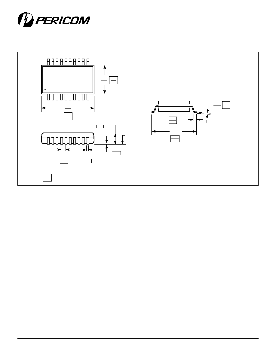
20-Pin SOIC Package Drawing (S)
20-Pin QSOP Package Drawing (Q)
9
PS7007B 01/13/99
12345678901234567890123456789012123456789012345678901234567890121234567890123456789012345678901212345678901234567890123456789012123456789012
PI49FCT3805/3806
3.3V Fast CMOS Buffer/Clock Driver
Pericom Semiconductor Corporation
2380 Bering Drive ∑ San Jose, CA 95131 ∑ 1-800-435-2336 ∑ Fax (408) 435-1100 ∑ http://www.pericom.com
20-Pin SSOP Package Drawing (H)
.272
.295
.078
.002
SEATING
PLANE
.0098
Max.
.0256
BSC
.022
.037
.004
.009
.291
.322
1
20
.197
.220
0.25
X.XX
X.XX
DENOTES DIMENSIONS
IN MILLIMETERS
0.050
7.40
8.20
0.55
0.95
0.09
0.25
5.00
5.60
2.00
6.90
7.50
0.65
Max
Min