 | ÐлекÑÑоннÑй компоненÑ: PI6C104S | СкаÑаÑÑ:  PDF PDF  ZIP ZIP |
Äîêóìåíòàöèÿ è îïèñàíèÿ www.docs.chipfind.ru
234
12345678901234567890123456789012123456789012345678901234567890121234567890123456789012345678901212345678901234567890123456789012123456789012
12345678901234567890123456789012123456789012345678901234567890121234567890123456789012345678901212345678901234567890123456789012123456789012
12345678901234567890123456789012123456789012345678901234567890121234567890123456789012345678901212345678901234567890123456789012123456789012
PS8164B 03/15/99
PI6C104
Spread Spectrum Clock Synthesizer
for Desktop Pentium II
PCICLK_F/S1
PCICLK1
VSS
PCICLK3
PCICLK4
PCICLK2
PCICLK5
PCICLK6/PD#
VDD
48M/MODE
24M/REF/S2
VSS
VDD
VDD2
VDD2
CPUCLK0
CPUCLK1
VDD
VSS
SDATA
SCLK
S0
VSS
1
2
3
4
5
6
7
8
9
10
11
12
13
14
28
27
26
25
24
23
22
21
20
19
18
17
16
15
XTAL_IN
XTAL_OUT
VDD
APIC
REF1/P14
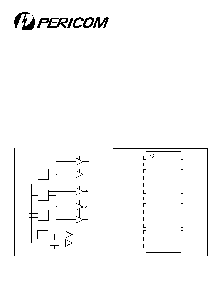
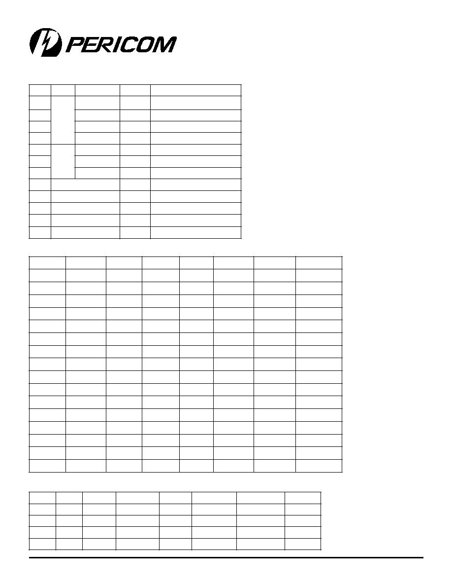
Pin Configuration
Block Diagram
Features
·
Up to 112 MHz operation
·
Spread Spectrum Modulation for CPUCLK, and PCICLK
·
Two copies of CPU clock with V
DD
of 2.5V ±5%
·
Seven copies of PCI clock,
(synchronous with CPU clock) 3.3V
·
One copy of Ref. clock @ 14.31818MHz (3.3V
TTL
)
·
48MHz USB Clock, 24MHz Super I/O clock
·
I
2
C Serial Configuration Interface
·
Low cost 14.31818MHz crystal oscillator input
·
Power management control
·
Isolated core V
DD
, V
SS
pins for noise reduction
·
28-pin SSOP (H) and SOIC package (S)
Description
The PI6C104 is a high-speed low-noise clock generator designed
to work with the PI6C18X family of clock buffer to meet all clock
needs for Desktop Intel Architecture platforms. CPU and chipset
clock frequencies from 66.6 MHz to 112 MHz are supported.
Split supplies of 3.3V and 2.5V are used. The 3.3V power supply
powers a portion of the I/O and the core. The 2.5V is used to power
the remaining outputs (CPU and APIC). 2.5V signaling follows
JEDEC standard 8-X. Power sequencing of the 3.3V and 2.5V
supplies is not required.
An asynchronous PD# signal may be used to orderly power down
(or up) the system during power on.
28-Pin
H, S
REF1
APIC
V
DDREF
V
DDAPIC
PCICLK[1:6]
CPUCLK[0:1]
REF
OSC
V
DDCPU
2
6
V
DDPCI
0,1
PCICLK_F
Div
PLL1
SEL
XTAL_OUT
XTAL_IN
S[0..2]
S
DATA
SCLOCK
I
2
C
PLL2
V
DDP
2
PI4
48MHz
24MHz/REF
MUX
235
12345678901234567890123456789012123456789012345678901234567890121234567890123456789012345678901212345678901234567890123456789012123456789012
12345678901234567890123456789012123456789012345678901234567890121234567890123456789012345678901212345678901234567890123456789012123456789012
12345678901234567890123456789012123456789012345678901234567890121234567890123456789012345678901212345678901234567890123456789012123456789012
PS8164B 03/15/99
PI6C104
Spread Spectrum Clock Synthesizer
for Desktop Pentium II
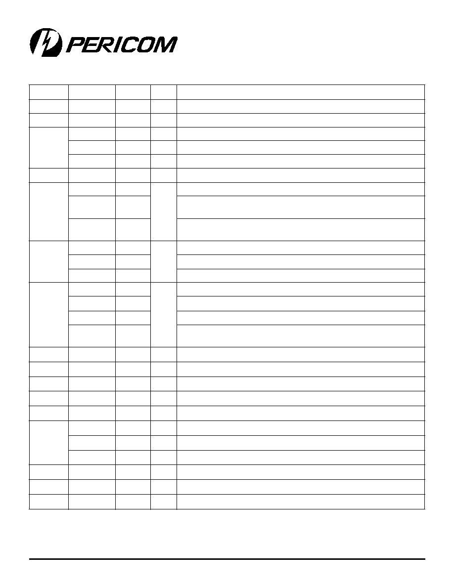
Pin Description
n
i
P
e
m
a
N
l
a
n
g
i
S
e
p
y
T
.
y
t
Q
n
o
it
p
i
r
c
s
e
D
1
N
I
_
L
A
T
X
I
X
1
t
u
p
n
i
l
a
t
s
y
r
c
z
H
M
8
1
3
.
4
1
2
T
U
O
_
L
A
T
X
O
X
1
t
u
p
n
i
l
a
t
s
y
r
c
z
H
M
8
1
3
.
4
1
4
F
_
K
L
C
I
C
P
O
1
.t
u
p
t
u
o
k
c
o
l
c
I
C
P
g
n
i
n
n
u
r
e
e
r
F
1
S
U
P
+
I
1
ti
b
t
c
el
e
S
y
c
n
e
u
q
e
r
F
e
si
w
r
e
h
t
o
t
u
p
t
u
o
F
_
K
L
C
I
C
P
,t
u
p
n
i
1
S
si
n
i
p
si
h
t
p
u
r
e
w
o
p
g
n
ir
u
D
0
1
,
8
,
7
,
6
,
5
]
5
:
1
[
K
L
C
I
C
P
O
5
.s
t
u
p
t
u
o
k
c
o
l
c
I
C
P
1
1
6
K
L
C
I
C
P
O
1
.s
t
u
p
t
u
o
k
c
o
l
c
I
C
P
#
D
P
U
P
+
I
n
e
h
w
d
el
b
a
si
d
e
r
a
s
k
c
o
l
c
U
P
C
d
n
a
I
C
P
.t
u
p
n
i
n
w
o
D
r
e
w
o
P
w
o
l
e
v
it
c
A
F
_
K
L
C
I
C
P
r
o
f
t
p
e
c
x
e
,
w
o
l
si
#
D
P
,t
u
p
n
i
#
D
P
:
0
=
E
D
O
M
.)
3
1
n
i
p
(
E
D
O
M
y
b
t
e
s
si
n
i
p
si
h
T
t
u
p
t
u
o
6
K
L
C
I
C
P
:
1
=
E
D
O
M
3
1
M
8
4
O
1
t
u
p
t
u
o
z
H
M
8
4
E
D
O
M
U
P
+
I
t
u
p
t
u
o
6
K
L
C
I
C
P
=
1
,t
u
p
n
i
#
D
P
=
0
,
1
1
n
i
p
f
o
n
o
it
i
n
if
e
d
e
h
t
s
e
n
i
m
r
e
t
e
d
E
D
O
M
p
u
r
e
w
o
p
r
e
tf
a
t
u
p
t
u
o
z
H
M
8
4
s
e
m
o
c
e
B
.
p
u
r
e
w
o
p
g
n
ir
u
d
d
el
p
m
a
s
,t
u
p
n
i
n
a
a
si
si
h
T
4
1
M
4
2
O
1
t
u
p
t
u
o
z
H
M
4
2
F
E
R
O
.t
u
p
t
u
o
e
c
n
e
r
e
f
e
R
d
e
r
e
ff
u
B
2
S
U
P
+
I
.
2
ti
b
t
c
el
e
S
y
c
n
e
u
q
e
r
F
:
st
c
el
e
s
e
d
o
m
)
7
2
n
i
p
(
4
1
P
.
e
si
w
r
e
h
t
o
t
u
p
t
u
o
,t
u
p
n
i
2
S
si
n
i
p
si
h
t
p
u
r
e
w
o
p
g
n
ir
u
D
z
H
M
4
2
=
1
,
F
E
R
=
0
6
1
0
S
U
P
+
I
1
0
ti
b
t
c
el
e
S
y
c
n
e
u
q
e
r
F
7
1
K
L
C
S
U
P
+
I
1
I
r
o
f
k
c
o
l
C
l
ai
r
e
S
2
e
c
a
fr
e
t
n
i
C
8
1
A
T
A
D
S
U
P
+
O
I
1
I
r
o
f
a
t
a
D
l
ai
r
e
S
2
e
c
a
fr
e
t
n
i
C
2
2
,
1
2
]
1
:
0
[
K
L
C
U
P
C
O
2
t
u
p
t
u
o
k
c
o
l
c
U
P
C
4
2
C
I
P
A
O
1
.t
u
p
t
u
o
l
a
t
s
y
r
C
d
e
r
e
ff
u
B
7
2
1
F
E
R
O
1
.t
u
p
t
u
o
l
a
t
s
y
r
C
d
e
r
e
ff
u
B
4
1
P
1
1
z
H
M
4
2
=
1
,
1
F
E
R
=
0
,t
c
el
e
s
e
d
o
m
4
1
n
i
P
.
e
si
w
r
e
h
t
o
t
u
p
t
u
o
1
F
E
R
,t
u
p
n
i
4
1
P
si
n
i
p
si
h
t
p
u
r
e
w
o
p
g
n
ir
u
D
6
2
,
0
2
,
2
1
,
9
V
D
D
4
V
3
.
3
.
L
L
P
,
F
E
R
,
e
r
o
C
,I
C
P
r
o
f
y
l
p
p
u
s
r
e
w
o
P
5
2
,
3
2
V
2
D
D
2
V
5
.
2
.s
k
c
o
l
c
U
P
C
&
C
I
P
A
r
o
f
y
l
p
p
u
s
r
e
w
o
P
8
2
,
9
1
,
5
1
,
3
V
S
S
4
s
d
n
u
o
r
G
236
12345678901234567890123456789012123456789012345678901234567890121234567890123456789012345678901212345678901234567890123456789012123456789012
12345678901234567890123456789012123456789012345678901234567890121234567890123456789012345678901212345678901234567890123456789012123456789012
12345678901234567890123456789012123456789012345678901234567890121234567890123456789012345678901212345678901234567890123456789012123456789012
PS8164B 03/15/99
PI6C104
Spread Spectrum Clock Synthesizer
for Desktop Pentium II
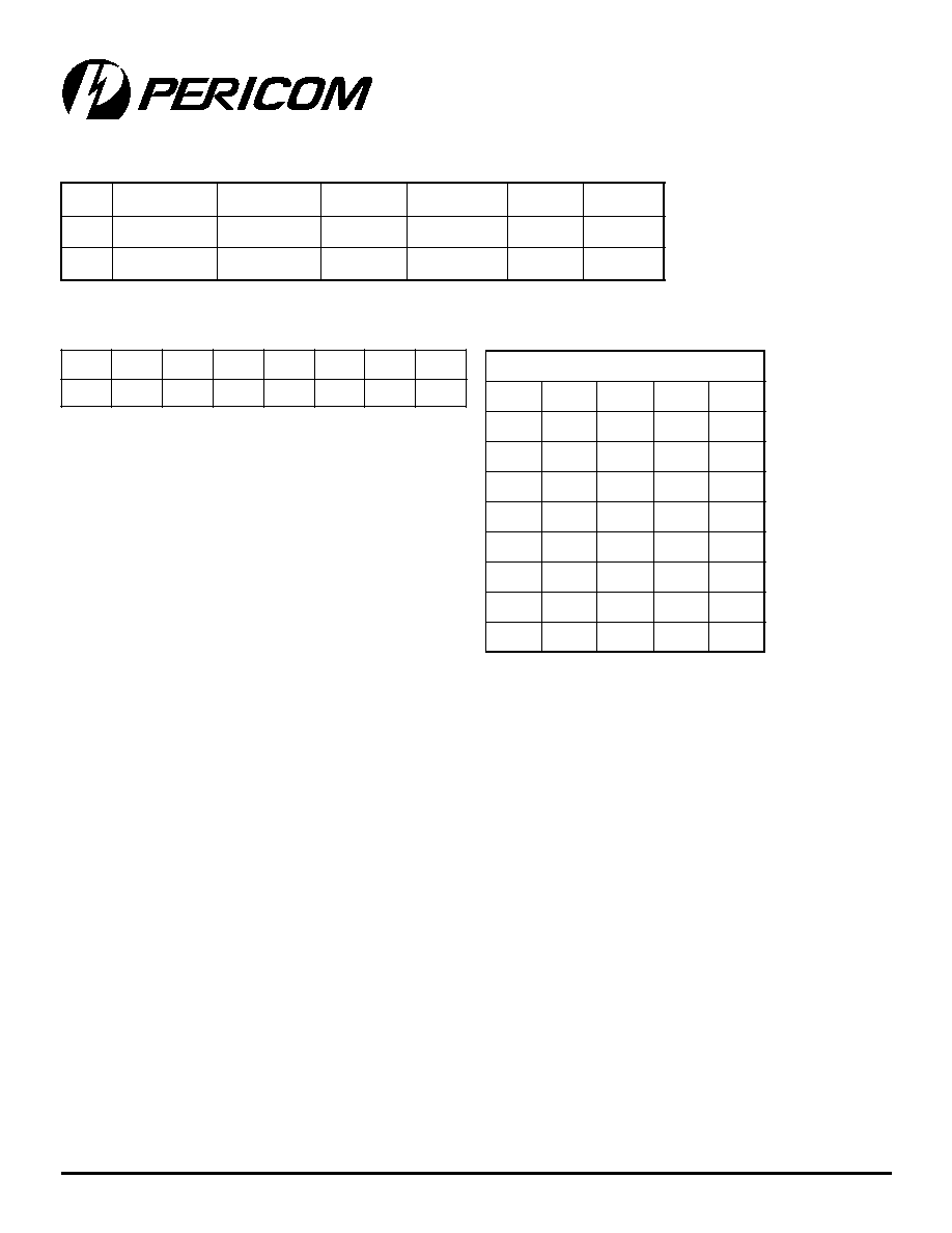
PI6C104 I
2
C Address Assignment 0D2H
2-Wire I
2
C Control
The I
2
C interface permits individual enable/disable of each clock
output and test mode enable.
The PI6C104 is a slave receiver device. It can not be read back. Sub
addressing is not supported. All preceding bytes must be sent in
order to change one of the control bytes.
Every byte put on the SDATA line must be 8-bits long (MSB first),
followed by an acknowledge bit generated by the receiving device.
During normal data transfers SDATA changes only when SCLK is
LOW. Exceptions: A HIGH to LOW transition on SDATA while
SCLK is HIGH indicates a start condition. A LOW to HIGH
transition on SDATA while SCLK is HIGH is a stop condition
and indicates the end of a data transfer cycle.
Each data transfer is initiated with a start condition and ended
with a stop condition. The first byte after a start condition is always
a 7-bit address byte followed by a read/write bit. (HIGH = read
from addressed device, LOW = write to addressed device).
If the devices own address is detected, PI6C104 generates an
acknowledge by pulling SDATA line LOW during ninth clock
pulse, then accepts the following data bytes until another start or
stop condition is detected.
Following acknowledgement of the address byte (D2), two more
bytes must be sent:
1. Command Code byte, and
2. Byte Count byte.
Although the data bits on these two bytes are dont care, they
must be sent and acknowledged.
7
A
6
A
5
A
4
A
3
A
2
A
1
A
0
A
1
1
0
1
0
0
1
0
Clock Enable Configuration
#
D
P
]
1
:
0
[
K
L
C
U
P
C
]
5
:
1
[
K
L
C
I
C
P
F
_
K
L
C
I
C
P
s
k
c
o
l
C
r
e
h
t
O
l
a
t
s
y
r
C
s'
O
C
V
0
w
o
l
w
o
l
g
n
i
n
n
u
R
g
n
i
n
n
u
R
g
n
i
n
n
u
R
g
n
i
n
n
u
R
1
g
n
i
n
n
u
R
g
n
i
n
n
u
R
g
n
i
n
n
u
R
g
n
i
n
n
u
R
g
n
i
n
n
u
R
g
n
i
n
n
u
R
e
l
b
a
T
y
c
n
e
u
q
e
r
F
0
S
1
S
2
S
U
P
C
I
C
P
0
0
0
5
7
0
3
0
0
1
8
.
6
6
4
.
3
3
0
1
0
6
.
6
6
3
.
3
3
0
1
1
8
.
6
6
4
.
3
3
1
0
0
2
1
1
3
.
7
3
1
0
1
3
.
3
8
3
.
3
3
1
1
0
0
0
1
3
.
3
3
1
1
1
0
0
1
3
.
3
3
237
12345678901234567890123456789012123456789012345678901234567890121234567890123456789012345678901212345678901234567890123456789012123456789012
12345678901234567890123456789012123456789012345678901234567890121234567890123456789012345678901212345678901234567890123456789012123456789012
12345678901234567890123456789012123456789012345678901234567890121234567890123456789012345678901212345678901234567890123456789012123456789012
PS8164B 03/15/99
PI6C104
Spread Spectrum Clock Synthesizer
for Desktop Pentium II
Byte 3 : Frequency, Spread Spectrum
Byte 4 : Clock Controls (1 = Enabled, 0 = Disabled)
#
ti
B
p
u
P
#
n
i
P
e
m
a
N
n
o
it
p
i
r
c
s
e
D
7
0
~
D
V
S
R
d
e
v
r
e
s
e
R
6
~
0
S
0
ti
B
t
c
el
e
S
y
c
n
e
u
q
e
r
F
5
~
1
S
1
ti
B
t
c
el
e
S
y
c
n
e
u
q
e
r
F
4
~
2
S
2
ti
B
t
c
el
e
S
y
c
n
e
u
q
e
r
F
3
~
S
F
S
t
c
el
e
S
y
c
n
e
u
q
e
r
F
e
r
a
w
d
r
a
H
=
0
1
(
t
c
el
e
S
y
c
n
e
u
q
e
r
F
e
r
a
w
tf
o
S
=
1
2
).
g
e
r
C
2
~
D
V
S
R
d
e
v
r
e
s
e
R
1
~
1
E
D
O
M
1
ti
B
e
d
o
M
0
~
0
E
D
O
M
0
ti
B
e
d
o
M
1
M
0
M
0
0
ff
O
m
u
rt
c
e
p
S
d
a
e
r
p
S
0
1
e
d
o
M
t
s
e
T
1
0
n
O
m
u
rt
c
e
p
S
d
a
e
r
p
S
1
1
Z
-i
H
Byte 5 : PCI Clock Control (1 = Enabled, 0 = Disabled)
#
ti
B
p
u
P
#
n
i
P
e
m
a
N
n
o
it
p
i
r
c
s
e
D
7
0
~
D
V
S
R
d
e
v
r
e
s
e
R
6
~
5
~
4
~
3
~
2
1
1
2
N
E
1
U
P
C
el
b
a
n
E
si
tl
u
a
f
e
D
,
el
b
a
n
E
1
K
L
C
U
P
C
1
0
~
D
V
S
R
d
e
v
r
e
s
e
R
0
1
2
2
N
E
0
U
P
C
el
b
a
n
E
si
tl
u
a
f
e
D
,
el
b
a
n
E
0
K
L
C
U
P
C
#
ti
B
p
u
P
#
n
i
P
e
m
a
N
n
o
it
p
i
r
c
s
e
D
7
1
4
N
E
F
I
C
P
el
b
a
n
E
si
tl
u
a
f
e
D
,
el
b
a
n
E
F
_
I
C
P
6
0
1
1
N
E
6
I
C
P
el
b
a
n
E
si
tl
u
a
f
e
D
,
el
b
a
n
E
6
I
C
P
5
1
0
1
N
E
5
I
C
P
el
b
a
n
E
si
tl
u
a
f
e
D
,
el
b
a
n
E
5
I
C
P
4
0
~
~
d
e
v
r
e
s
e
R
3
1
8
N
E
4
I
C
P
el
b
a
n
E
si
tl
u
a
f
e
D
,
el
b
a
n
E
4
I
C
P
2
7
N
E
3
I
C
P
el
b
a
n
E
si
tl
u
a
f
e
D
,
el
b
a
n
E
3
I
C
P
1
6
N
E
2
I
C
P
el
b
a
n
E
si
tl
u
a
f
e
D
,
el
b
a
n
E
2
I
C
P
0
5
N
E
1
I
C
P
el
b
a
n
E
si
tl
u
a
f
e
D
,
el
b
a
n
E
1
I
C
P
238
12345678901234567890123456789012123456789012345678901234567890121234567890123456789012345678901212345678901234567890123456789012123456789012
12345678901234567890123456789012123456789012345678901234567890121234567890123456789012345678901212345678901234567890123456789012123456789012
12345678901234567890123456789012123456789012345678901234567890121234567890123456789012345678901212345678901234567890123456789012123456789012
PS8164B 03/15/99
PI6C104
Spread Spectrum Clock Synthesizer
for Desktop Pentium II
Table 1: Byte 3 Frequency and Spread Spectrum Table
Byte 0: Test Mode Table
S
F
S
3
ti
B
N
E
S
S
1
ti
B
0
S
6
ti
B
1
S
5
ti
B
2
S
4
ti
B
)
z
H
M
(
U
P
C
)
z
H
M
(
I
C
P
)
%
(
d
a
e
r
p
S
1
0
0
0
0
5
7
0
3
F
F
O
1
0
0
0
1
8
.
6
6
4
.
3
3
F
F
O
1
0
0
1
0
6
.
6
6
3
.
3
3
F
F
O
1
0
0
1
1
8
.
6
6
4
.
3
3
F
F
O
1
0
1
0
0
2
1
1
3
.
7
3
F
F
O
1
0
1
0
1
3
.
3
8
3
.
3
3
F
F
O
1
0
1
1
0
0
0
1
3
.
3
3
F
F
O
1
0
1
1
1
0
0
1
3
.
3
3
F
F
O
1
1
0
0
0
5
7
0
3
5
.
0
+
~
5
.
0
-
1
1
0
0
1
8
.
6
6
4
.
3
3
9
.
0
+
~
9
.
0
-
1
1
0
1
0
6
.
6
6
3
.
7
3
0
.
0
+
~
0
.
1
-
1
1
0
1
1
8
.
6
6
4
.
3
3
5
.
0
+
~
5
.
0
-
1
1
1
0
0
2
1
1
3
.
7
3
5
.
0
+
~
5
.
0
-
1
1
1
0
1
3
.
3
8
3
.
3
3
5
.
0
+
~
5
.
0
-
1
1
1
1
0
0
0
1
3
.
3
3
0
.
0
+
~
1
-
1
1
1
1
1
0
0
1
3
.
3
3
0
.
0
+
~
5
.
0
-
1
ti
B
0
ti
B
U
P
C
I
C
P
M
8
4
M
4
2
C
I
P
A
/
F
E
R
e
d
o
M
0
0
1
el
b
a
t
1
el
b
a
t
z
H
M
8
4
f
e
R
/
z
H
M
4
2
z
H
M
8
1
3
.
4
1
l
a
m
r
o
N
0
1
2
/
n
i
X
6
/
n
i
X
2
/
n
i
X
4
/
n
i
X
n
i
X
t
s
e
T
1
0
1
el
b
a
t
1
el
b
a
t
z
H
M
8
4
f
e
R
/
z
H
M
4
2
z
H
M
8
1
3
.
4
1
C
S
S
1
1
Z
-i
H
Z
-i
H
Z
-i
H
Z
-i
H
Z
-i
H
e
t
a
t
s
-i
r
T
Byte 6 : REF Clock Control (1 = Enabled, 0 = Disabled)
#
ti
B
p
u
P
#
n
i
P
e
m
a
N
n
o
it
p
ir
c
s
e
D
7
0
~
D
V
S
R
d
e
v
r
e
s
e
R
6
~
D
V
S
R
d
e
v
r
e
s
e
R
5
4
2
N
E
C
I
P
A
el
b
a
n
E
si
tl
u
af
e
D
,e
l
b
a
n
E
C
I
P
A
4
~
D
V
S
R
d
e
v
r
e
s
e
R
2
1
~
D
V
S
R
d
e
v
r
e
s
e
R
1
6
2
1
N
E
F
R
1
el
b
a
n
E
e
vi
r
d
h
gi
H
1
F
E
R
0
6
2
0
N
E
F
R
0
el
b
a
n
E
e
vi
r
d
h
gi
H
1
F
E
R
0
N
E
F
R
1
N
E
F
R
0
0
e
vi
r
D
w
o
L
1
0
tl
u
af
e
D
,e
vi
r
D
l
a
m
r
o
N
0
1
e
vi
r
D
h
gi
H
1
1
Note: Outputs are disabled @ low state
Notes:
Bit 3 = Enable Software
Frequency Select
Bit 1 = Enable Software
Frequency Select
Bit 6 = Frequency Select 0
Bit 5 = Frequency Select 1
Bit 4 = Frequency Select 0