1
PS8410 08/11/99
REF/SEL2 1
V
DD3.3
2
XTAL_IN 3 3.3V
2.5V
2.5V
3.3V
3.3V
3.3V
XTAL_OUT 4
V
SS3.3
5
V
SS3.3
6
3V66 0 7
3V66 1 8
V
DD3.3
9
V
DD3.3
10
PCI 0 11
PCI 1 12
PCI 2 13
V
SS3.3
14
PCI 3 15
PCI 4 16
V
SS3.3
17
PCI 5 18
PCI 6 19
PCI 7 20
V
DD3.3
21
V
DDA
22
V
SSA
23
V
SS3.3
24
48MHz0 25
48MHz1 26
V
DD3.3
27
SEL0 28
V
SS2.5
APIC0
APIC1
V
DD2.5
CPU 0
V
DD2.5
CPU 1
CPU 2
V
SS2.5
56
V
SS3.3
55
SDRAM0
54
SDRAM1
53
V
DD3.3
52
SDRAM2
51
SDRAM3
50
V
SS3.3
49
SDRAM4
48
SDRAM5
47
V
DD3.3
46
SDRAM6
45
SDRAM7
44
V
SS3.3
43
DCLK
42
V
DD3.3
41
40
39
38
37
36
35
34
33
PWR_DWN#
SCLK
SDATA
SEL1
32
31
30
29
3.3V
56-Pin
(V56)
DCLK
REF
OSC
REF
XIN
XOUT
48 MHz 0-1
3V66 0-1
PCI 0-7
SDRAM 0-7
CPU 0-2
PLL2
PLL1
2
2
APIC 0-1
2
3
8
8
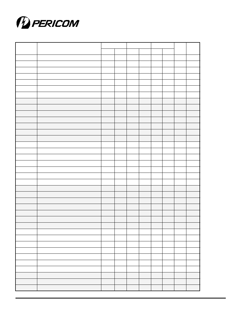
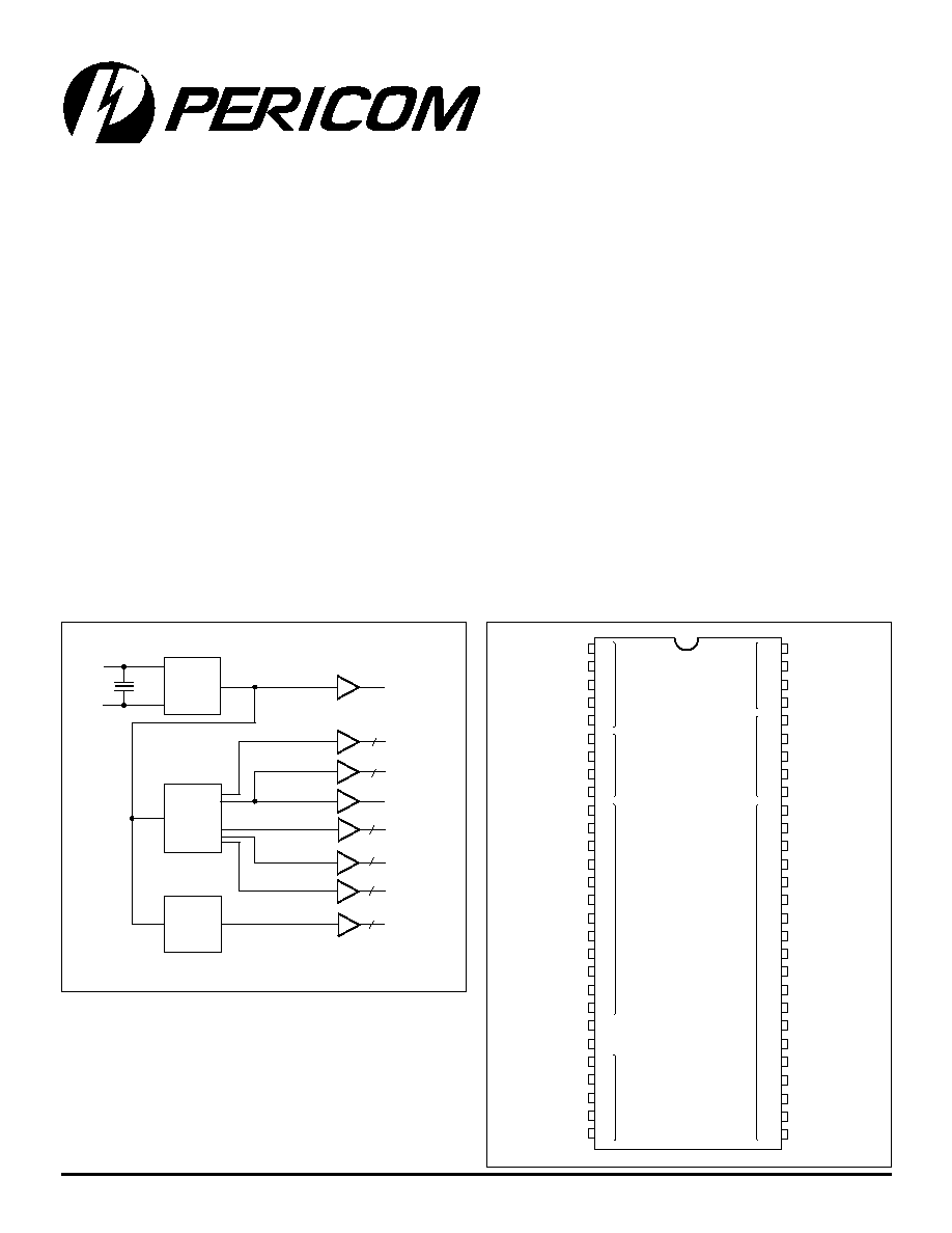
Pin Configuration
12345678901234567890123456789012123456789012345678901234567890121234567890123456789012345678901212345678901234567890123456789012123456789012
12345678901234567890123456789012123456789012345678901234567890121234567890123456789012345678901212345678901234567890123456789012123456789012
12345678901234567890123456789012123456789012345678901234567890121234567890123456789012345678901212345678901234567890123456789012123456789012
PI6C110E
Clock Solution for 133 MHz
Celeron/Pentium II/III Processors
Block Diagram
Features
3 of 2.5V 66/100/133 MHz CPU (CPU[0-2])
2 of 2.5V 33 MHz APIC (APIC[0-1])
9 of 3.3V 100/133 MHz SDRAM (SDRAM[0-7], DCLK)
8 of 3.3V 33 MHz PCI (PCI[0-7])
2 of 3.3V 66 MHz (3V66 [0-1])
2 of 3.3V 48 MHz (48MHz [0-1])
1 of 3.3V 14.3 MHz (REF)
Selectable CPU and SDRAM clocks (on power up only)
Power down function using PWR_DWN#
Spread Spectrum Enable/Disable by I
2
C
I
2
C interface to turn off unused clocks
56 pin SSOP package (V)
Description
Pericom PI6C110E integrates a dual PLL clock generator, SDRAM
buffer and I
2
C interface. The clock generator section comprised
of an oscillator, 2 low jitter phased locked loop, skew control, and
power down logic. The SDRAM buffers are high speed and low
skew to handle data transfers in excess of 133 MHz.
When Spread Spectrum mode is enabled, all clock outputs are
modulated except for REF and 48 MHz[0-1] outputs. These clocks
are down spread linearly (triangular modulation) by +0%, 0.6%.
To minimize power consumption and EMI radiation some unused
outputs can be turned off. Two wire I
2
C interface is used to enable/
disable Spread Spectrum mode, and to turned off PCI clocks, CPU
clocks, and 48 MHz clocks.
For low power sleep mode, the entire device can be placed to power
down mode. Driving the PWR_DWN# to low state disables the
entire chip. In this state the crystal oscillator, and both PLLs are
turned off. Furthermore, all outputs are deactivated to low state, all
inputs are inactive except for PWR_DWN#.
All trademarks are of their respective companies.
V
2
PS8410 08/11/99
12345678901234567890123456789012123456789012345678901234567890121234567890123456789012345678901212345678901234567890123456789012123456789012
12345678901234567890123456789012123456789012345678901234567890121234567890123456789012345678901212345678901234567890123456789012123456789012
PI6C110E
Clock Solution for 133 MHz
Celeron/Pentium II/III Processors
n
i
P
e
p
y
T
.
y
t
Q
S
/
P
l
o
b
m
y
S
n
o
it
p
i
r
c
s
e
D
1
O
/I
1
3
.
3
2
L
E
S
/
F
E
R
si
n
i
p
si
h
t
p
u
r
e
w
o
p
g
n
ir
u
D
.t
u
p
t
u
o
e
c
n
e
r
e
f
e
r
z
H
M
8
1
3
.
4
1
y
ll
a
m
r
o
N
.
m
h
O
K
0
0
1
/
w
n
w
o
d
d
el
l
u
p
y
ll
a
n
r
e
t
n
I
.
2
ti
b
k
c
o
l
c
,
2
L
E
S
s
a
d
el
p
m
a
s
3
I
1
3
.
3
N
I
_
L
A
T
X
t
u
p
n
i
l
a
t
s
y
r
c
z
H
M
8
1
3
.
4
1
4
O
1
3
.
3
T
U
O
_
L
A
T
X
t
u
p
t
u
o
l
a
t
s
y
r
c
z
H
M
8
1
3
.
4
1
8
,
7
O
2
3
.
3
]
1
-
0
[
6
6
V
3
z
H
M
6
6
,
5
1
,
3
1
,
2
1
,
1
1
0
2
,
9
1
,
8
1
,
6
1
O
8
3
.
3
]
7
-
0
[
I
C
P
st
u
p
t
u
o
I
C
P
6
2
,
5
2
O
1
3
.
3
]
1
-
0
[
z
H
M
8
4
t
u
p
t
u
o
z
H
M
8
4
9
2
,
8
2
I
2
3
.
3
]
1
-
0
[
L
E
S
p
u
ll
u
p
l
a
n
r
e
t
n
i
,s
t
u
p
n
i
t
c
el
e
s
y
c
n
e
u
q
e
rf
l
e
v
el
L
T
T
V
L
0
3
O
/I
1
3
.
3
A
T
A
D
S
I
2
p
u
ll
u
p
l
a
n
r
e
t
n
i
,
A
T
A
D
S
el
b
it
a
p
m
o
c
C
1
3
I
1
3
.
3
K
C
O
L
C
S
I
2
p
u
ll
u
p
l
a
n
r
e
t
n
i
,
K
C
O
L
C
S
el
b
it
a
p
m
o
c
C
2
3
I
1
3
.
3
#
N
W
D
R
W
P
w
o
l
e
v
it
c
a
,t
u
p
n
i
l
o
rt
n
o
c
n
w
o
D
r
e
w
o
P
l
e
v
el
L
T
T
V
L
,
9
3
,
7
3
,
6
3
,
4
3
6
4
,
5
4
,
3
4
,
2
4
,
0
4
O
9
3
.
3
,
K
L
C
D
]
7
-
0
[
M
A
R
D
S
.]
2
-
0
[
L
E
S
n
o
g
n
i
d
n
e
p
e
d
z
H
M
3
3
1
/
0
0
1
.s
t
u
p
t
u
o
K
L
C
D
d
n
a
M
A
R
D
S
I
h
g
u
o
r
h
t
ff
o
d
e
n
r
u
t
e
b
n
a
c
]
7
-
0
[
M
A
R
D
S
2
.
K
L
C
D
t
o
n
t
u
b
,
C
2
5
,
0
5
,
9
4
O
3
5
.
2
]
2
-
0
[
U
P
C
]
2
-
0
[
L
E
S
n
o
g
n
i
d
n
e
p
e
d
z
H
M
3
3
1
/
0
0
1
/
6
6
.t
u
p
t
u
o
k
c
o
l
C
s
u
B
t
s
o
H
5
5
,
4
5
O
2
5
.
2
]
1
-
0
[
C
I
P
A
k
c
o
l
c
I
C
P
o
t
s
u
o
n
o
r
h
c
n
y
s
,
k
c
o
l
c
C
I
P
A
z
H
M
3
3
,
7
2
,
1
2
,
0
1
,
9
,
2
4
4
,
8
3
,
3
3
R
W
P
8
3
.
3
V
3
.
3
D
D
y
l
p
p
u
S
r
e
w
o
P
V
3
.
3
,
4
2
,
7
1
,
4
1
,
6
,
5
7
4
,
1
4
,
5
3
D
N
G
8
A
/
N
V
3
.
3
S
S
d
n
u
o
r
G
V
3
.
3
3
5
,
1
5
R
W
P
2
5
.
2
V
5
.
2
D
D
y
l
p
p
u
S
r
e
w
o
P
V
5
.
2
6
5
,
8
4
D
N
G
2
A
/
N
V
5
.
2
S
S
d
n
u
o
r
G
V
5
.
2
2
2
R
W
P
1
3
.
3
V
A
D
D
y
l
p
p
u
S
r
e
w
o
P
e
r
o
C
V
3
.
3
3
2
D
N
G
1
A
/
N
V
A
S
S
d
n
u
o
r
G
e
r
o
C
V
3
.
3
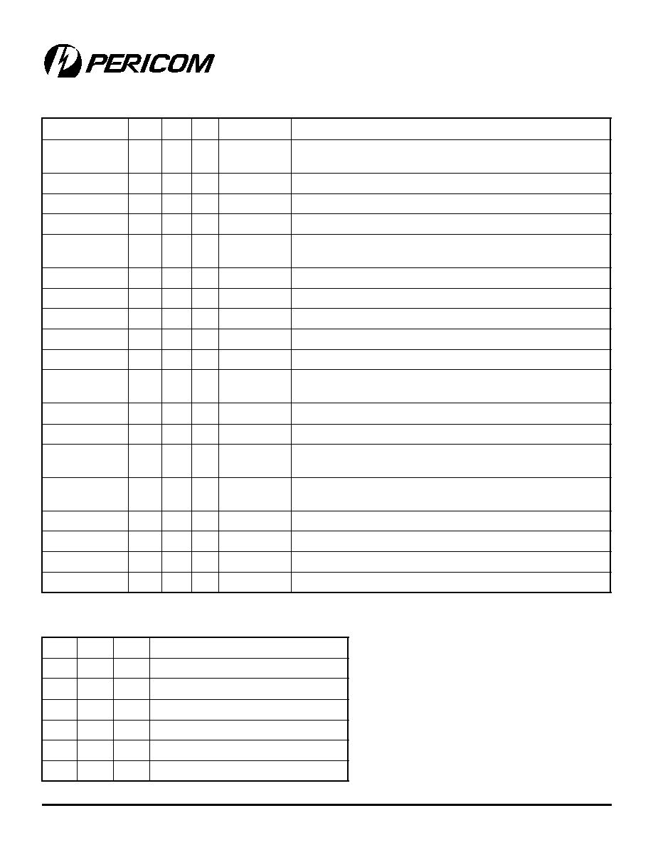
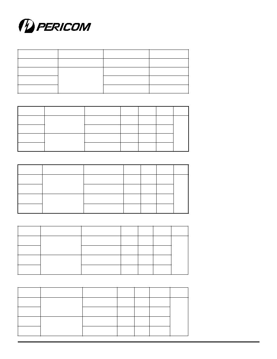
Pin Description Table
2
L
E
S
1
L
E
S
0
L
E
S
n
o
it
c
n
u
F
X
0
0
e
t
a
t
S
-i
r
T
X
0
1
t
s
e
T
0
1
0
z
H
M
0
0
1
=
M
A
R
D
S
,z
H
M
6
6
=
U
P
C
0
1
1
z
H
M
0
0
1
=
M
A
R
D
S
,z
H
M
0
0
1
=
U
P
C
1
1
0
z
H
M
3
3
1
=
M
A
R
D
S
,z
H
M
3
3
1
=
U
P
C
1
1
1
z
H
M
0
0
1
=
M
A
R
D
S
,z
H
M
3
3
1
=
U
P
C
Frequency Select Function Table
3
PS8410 08/11/99
12345678901234567890123456789012123456789012345678901234567890121234567890123456789012345678901212345678901234567890123456789012123456789012
12345678901234567890123456789012123456789012345678901234567890121234567890123456789012345678901212345678901234567890123456789012123456789012
PI6C110E
Clock Solution for 133 MHz
Celeron/Pentium II/III Processors
Symbol
Parameter
Min.
Max.
Units
Notes
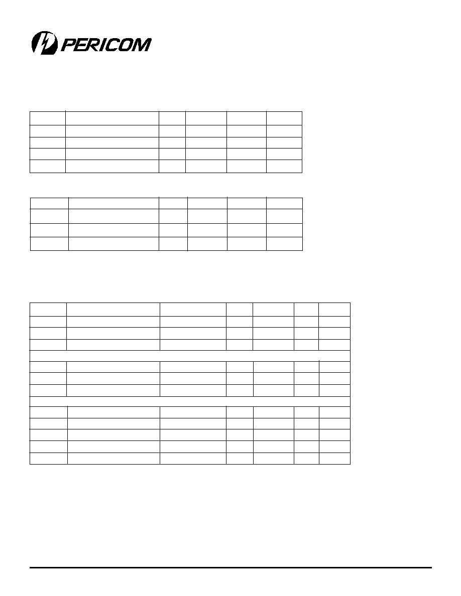
V
IH3
3.3V Input High Voltage
-0.5
4.6
V
1
V
IL3
3.3V Input Low Voltage
-0.5
V
ESD prot.
Input ESD protection
2000
V
2
DC Specifications
DC parameters must be sustainable under steady state (DC) conditions.
Notes:
1. Maximum V
IH
is not to exceed maximum V
DD
.
2. Human body model.
Symbol
Parameter
Min.
Max.
Units
Notes
V
DDA
3.3V Core Supply Voltage
-0.5
4.6
V
V
DD2.5
2.5V I/O Supply Voltage
-0.5
3.6
V
V
DD3.3
3.3V I/O Supply Voltage
-0.5
4.6
V
T
S
Storage Temperature
-65
150
�C
Absolute Maximum DC Power Supply
Absolute Maximum DC I/O
Symbol
Parameter
Condition
Min.
Max.
Units Notes
V
DDA
3.3V Core Supply Voltage
3.3V �5%
3.135
3.465
V
2
V
DD3.3
3.3V I/O Supply Voltage
3.3V �5%
3.135
3.465
V
2
V
DD2.5
2.5V I/O Supply Voltage
2.5V �5%
2.375
2.625
V
2
V
IH3
3.3V Input High Voltage
V
DDA
2.0 V
DD
+0.3 V
4
V
IL3
3.3V Input Low Voltage
V
SS
-0.3
0.8
V
4
I
IL
Input Leakage Current 0 <V
IN
<V
DD3.3
-5
+5
�
A
1,4
C
in
Input Pin Capacitance
5
pF
C
xtal
Xtal Pin Capacitance
13.5
22.5
pF
3
C
out
Output Pin Capacitance
6
pF
L
PIN
Pin Inductance
7
nH
T
A
Ambient Temperature
No Airflow
0
70
�C
DC Operating Specification
Notes:
1. Input Leakage Current does not include inputs with Pull-Up or Pull-down resistors.
2. No power sequencing is implied or allowed to be required in the system.
3. As seen by the crystal. Device is intended to be used with a 17-20pF AT crystal.
4. All inputs referenced to 3.3V power supply.
4
PS8410 08/11/99
12345678901234567890123456789012123456789012345678901234567890121234567890123456789012345678901212345678901234567890123456789012123456789012
12345678901234567890123456789012123456789012345678901234567890121234567890123456789012345678901212345678901234567890123456789012123456789012
PI6C110E
Clock Solution for 133 MHz
Celeron/Pentium II/III Processors
Clock Output Buffer DC Characteristics
e
m
a
N
r
e
ff
u
B
V
C
C
)
V
(
e
g
n
a
R
)
m
h
O
(
e
c
n
a
d
e
p
m
I
e
p
y
T
r
e
ff
u
B
C
I
P
A
,
U
P
C
5
2
6
.
2
-
5
7
3
.
2
5
4
-
5
.
3
1
1
e
p
y
T
F
E
R
,z
H
M
8
4
5
6
4
.
3
-
5
3
1
.
3
0
6
-
0
2
3
e
p
y
T
M
A
R
D
S
4
2
-
0
1
4
e
p
y
T
6
6
V
3
,I
C
P
5
5
-
2
1
5
e
p
y
T
l
o
b
m
y
S
r
e
t
e
m
a
r
a
P
n
o
it
i
d
n
o
C
.
n
i
M
.
p
y
T
.
x
a
M
s
ti
n
U
I
N
I
M
H
O
t
n
e
rr
u
C
p
U
-l
l
u
P
V
T
U
O
=
V
0
.
1
7
2
A
m
I
X
A
M
H
O
V
T
U
O
=
V
5
7
3
.
2
7
2
I
N
I
M
L
O
t
n
e
rr
u
C
n
w
o
D
-l
l
u
P
V
T
U
O
=
V
2
.
1
0
3
I
X
A
M
L
O
V
T
U
O
=
V
3
.
0
0
3
Type 1: CPU, APIC Clocks
l
o
b
m
y
S
r
e
t
e
m
a
r
a
P
n
o
it
i
d
n
o
C
.
n
i
M
.
p
y
T
.
x
a
M
s
ti
n
U
I
N
I
M
H
O
t
n
e
rr
u
C
p
U
-l
l
u
P
V
T
U
O
=
V
0
.
1
9
2
A
m
I
X
A
M
H
O
V
T
U
O
=
V
5
3
1
.
3
3
2
I
N
I
M
L
O
t
n
e
rr
u
C
n
w
o
D
-l
l
u
P
V
T
U
O
=
V
5
9
.
1
9
2
I
X
A
M
L
O
V
T
U
O
=
V
4
.
0
7
2
Type 3: 48 MHz, REF Clocks
l
o
b
m
y
S
r
e
t
e
m
a
r
a
P
n
o
it
i
d
n
o
C
.
n
i
M
.
p
y
T
.
x
a
M
s
ti
n
U
I
N
I
M
H
O
t
n
e
rr
u
C
p
U
-l
l
u
P
V
T
U
O
V
0
.
2
=
4
5
A
m
I
X
A
M
H
O
V
T
U
O
V
5
3
1
.
3
=
6
4
I
N
I
M
L
O
t
n
e
rr
u
C
n
w
o
D
-l
l
u
P
V
T
U
O
V
0
.
1
=
4
5
I
X
A
M
L
O
V
T
U
O
V
4
.
0
=
3
5
Type 4: SDRAM Clocks
l
o
b
m
y
S
r
e
t
e
m
a
r
a
P
n
o
it
i
d
n
o
C
.
n
i
M
.
p
y
T
.
x
a
M
s
ti
n
U
I
N
I
M
H
O
t
n
e
rr
u
C
p
U
-l
l
u
P
V
T
U
O
=
V
0
.
1
3
3
A
m
I
X
A
M
H
O
V
T
U
O
=
V
5
3
1
.
3
3
3
I
N
I
M
L
O
t
n
e
rr
u
C
n
w
o
D
-l
l
u
P
V
T
U
O
=
V
5
9
.
1
0
3
I
X
A
M
L
O
V
T
U
O
=
V
4
.
0
8
3
Type 5: PCI, 3V66 Clocks