
1
PS8384D 06/26/01
Product Features
∑
10 MHz to 134 MHz operating range
∑
Zero input-output propagation delay, adjustable by external
capacitive load on FBK input
∑
Multiple configurations, see Available PI6C2308
Configurations table
∑
Input to output delay, less than 200ps
∑
Multiple low skew outputs
- Output-output skew less than 200ps
- Device-device skew less than 600ps
- Two banks of four outputs, Hi-Z by two select inputs
∑
Low Jitter, less than 200ps
∑
3.3V operation
∑
Space-saving Packages:
16-pin, 150-mil SOIC package (W16) (-1, -1H, -2, -3, -4, -6)
16-pin TSSOP package (L16) (-1, -1H)
∑
Available in industrial and commercial temperatures
Functional Description
Providing two banks of four outputs, the PI6C2308 is a 3.3V zero-
delay buffer designed to distribute clock signals in applications
including PC, workstation, datacom, telecom, and high-performance
systems. Each bank of four outputs can be controlled by the select
inputs as shown in the Select Input Decoding Table.
The PI6C2308 provides 8 copies of a clock signal that has 200ps
phase error compared to a reference clock. The skew between the
output clock signals for PI6C2308 is less than 200ps. When there
are no rising edges on the REF input, the PI6C2308 enters a power
down state. In this mode, the PLL is off and all outputs are Hi-Z.
This results in less than 12µA of current draw. The Select Input
Decoding Table shows additional examples when the PLL shuts
down. The PI6C2308 configuration table shows all available devices.
The base part, PI6C2308-1, provides output clocks in sync with a
reference clock. With faster rise and fall times, the PI6C2308-1H
is the high drive version of the PI6C2308-1. Depending on which
output drives the feedback pin, PI6C2308-2 provides 2X and 1X
clock signals on each output bank. The PI6C2308-3 allows the user
to obtain 4X and 2X frequencies on the outputs. The PI6C2308-4
provides 2X clock signals on all outputs. PI6C2308 (-1, -2, -3, -4) allows
bank B to be Hi-Z when all output clocks are not required.The
PI6C2308-6 allows bank B to switch from Reference clock to half
of the frequency of Reference clock using the control inputs S1 and
S2 if Bank A is connected to feedback FBK. In addition, using the
control inputs S1 and S2, the PI6C2308-6 allows bank A to switch
from Reference clock to 2X the frequency of Reference clock if
Bank B is connected to feedback FBK. For testing purposes, the
select inputs connect the input clock directly to outputs.
Block Diagrams
Pin Configuration PI6C2308 (1, 1H, 2, 3, 4, 6)
12345678901234567890123456789012123456789012345678901234567890121234567890123456789012345678901212345678901234567890123456789012123456789012
12345678901234567890123456789012123456789012345678901234567890121234567890123456789012345678901212345678901234567890123456789012123456789012
3.3V Zero-Delay Buffer
PI6C2308
1
2
3
V
DD
4
GND
5
CLKA2
6
CLKB2
7
S1
8
CLKB1
FBK
CLKA3
V
DD
CLKB4
CLKB3
S2
16
15
14
13
12
11
10
9
REF
CLKA1
GND
CLKA4
16-Pin
W, L
PLL
MUX
REF
S2
S1
Select Input
Decoding
FBK
CLKA1
CLKA2
CLKA3
CLKA4
CLKB2
CLKB3
CLKB4
CLKB1
PI6C2308-6
MUX
˜2
˜2
PLL
MUX
Extra Divider (-3, -4)
Extra Divider (-2,-3)
REF
S2
S1
Select Input
Decoding
FBK
CLKA1
CLKA2
CLKA3
CLKA4
CLKB2
CLKB3
CLKB4
CLKB1
PI6C2308 (-1, -1H, -2, -3, -4)
˜2

2
PS8384D 06/26/01
12345678901234567890123456789012123456789012345678901234567890121234567890123456789012345678901212345678901234567890123456789012123456789012
12345678901234567890123456789012123456789012345678901234567890121234567890123456789012345678901212345678901234567890123456789012123456789012
PI6C2308
3.3V Zero Delay Buffer
2
S
1
S
]
4
-
1
[
A
K
L
C
]
4
-
1
[
B
K
L
C
e
c
r
u
o
S
t
u
p
t
u
O
n
w
o
d
t
u
h
S
L
L
P
0
0
Z
-i
H
Z
-i
H
L
L
P
Y
0
1
n
e
v
ir
D
Z
-i
H
L
L
P
N
1
0
n
e
v
ir
D
n
e
v
ir
D
e
c
n
e
r
e
f
e
R
Y
1
1
n
e
v
ir
D
n
e
v
ir
D
L
L
P
N
Select Input Decoding for PI6C2308 (-1, -1H, -2, -3, -4)
e
c
i
v
e
D
m
o
r
F
k
c
a
b
d
e
e
F
y
c
n
e
u
q
e
r
F
A
k
n
a
B
y
c
n
e
u
q
e
r
F
B
k
n
a
B
1
-
8
0
3
2
C
6
I
P
B
k
n
a
B
r
o
A
k
n
a
B
e
c
n
e
r
e
f
e
R
e
c
n
e
r
e
f
e
R
H
1
-
8
0
3
2
C
6
I
P
B
k
n
a
B
r
o
A
k
n
a
B
e
c
n
e
r
e
f
e
R
e
c
n
e
r
e
f
e
R
2
-
8
0
3
2
C
6
I
P
A
k
n
a
B
e
c
n
e
r
e
f
e
R
2
/
e
c
n
e
r
e
f
e
R
2
-
8
0
3
2
C
6
I
P
B
k
n
a
B
e
c
n
e
r
e
f
e
R
X
2
e
c
n
e
r
e
f
e
R
3
-
8
0
3
2
C
6
I
P
A
k
n
a
B
e
c
n
e
r
e
f
e
R
X
2
e
c
n
e
r
e
f
e
R
3
-
8
0
3
2
C
6
I
P
B
k
n
a
B
e
c
n
e
r
e
f
e
R
X
4
e
c
n
e
r
e
f
e
R
X
2
4
-
8
0
3
2
C
6
I
P
B
k
n
a
B
r
o
A
k
n
a
B
e
c
n
e
r
e
f
e
R
X
2
e
c
n
e
r
e
f
e
R
X
2
6
-
8
0
3
2
C
6
I
P
A
k
n
a
B
e
c
n
e
r
e
f
e
R
2
/
e
c
n
e
r
e
f
e
R
r
o
e
c
n
e
r
e
f
e
R
6
-
8
0
3
2
C
6
I
P
B
k
n
a
B
e
c
n
e
r
e
f
e
R
X
2
r
o
e
c
n
e
r
e
f
e
R
e
c
n
e
r
e
f
e
R
Available PI6C2308 Configurations
2
S
1
S
]
4
-
1
[
A
K
L
C
]
4
-
1
[
B
K
L
C
e
c
r
u
o
S
t
u
p
t
u
O
n
w
o
d
t
u
h
S
L
L
P
0
0
Z
-i
H
Z
-i
H
L
L
P
Y
0
1
e
c
n
e
r
e
f
e
R
=
n
e
v
ir
D
2
/
e
c
n
e
r
e
f
e
R
=
n
e
v
ir
D
e
c
n
e
r
e
f
e
R
Y
1
0
L
L
P
=
n
e
v
ir
D
L
L
P
=
n
e
v
ir
D
L
L
P
N
1
1
L
L
P
=
n
e
v
ir
D
2
/
L
L
P
=
n
e
v
ir
D
L
L
P
N
Select Input Decoding for PI6C2308-6
3
PS8384D 06/26/01
12345678901234567890123456789012123456789012345678901234567890121234567890123456789012345678901212345678901234567890123456789012123456789012
12345678901234567890123456789012123456789012345678901234567890121234567890123456789012345678901212345678901234567890123456789012123456789012
PI6C2308
3.3V Zero Delay Buffer
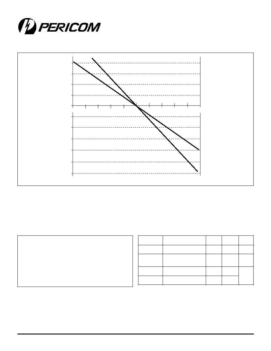
To close the feedback loop of the PI6C2308, the FBK pin can be
driven from any of the 8 available output pins. The output driving
the FBK pin will be driving a total load of 7pF plus any additional load
that it drives. The relative loading of this output (with respect to the
remaining outputs) can adjust the input-output delay. This is shown
in the graph above.
Zero Delay and Skew Control
REF. Input to CLKA/CLKB Delay vs. Difference in Loading between FBK pin and CLKA/CLKB pins
Maximum Ratings
Supply Voltage to Ground Potential ...................0.5V to +7.0V
DC Input Voltage (Except REF) ..................0.5V to V
DD
+0.5V
DC Input Voltage REF................................................ 0.5 to 7V
Storage Temperature ........................................ 65∫C to +150∫C
Maximum Soldering Temperature (10 seconds)................ 260∫C
Junction Temperature ....................................................... 150∫C
Static Discharge Voltage
(per MIL-STD-883, Method 3015).................................. >2000V
r
e
t
e
m
a
r
a
P
n
o
it
p
i
r
c
s
e
D
.
n
i
M
.
x
a
M
s
ti
n
U
V
D
D
e
g
a
tl
o
V
y
l
p
p
u
S
0
.
3
6
.
3
V
T
A
e
r
u
t
a
r
e
p
m
e
T
g
n
it
a
r
e
p
O
)t
n
ei
b
m
A
(
0
0
7
C
∫
C
L
e
c
n
a
ti
c
a
p
a
C
d
a
o
L
0
3
F
p
C
N
I
e
c
n
a
ti
c
a
p
a
C
t
u
p
n
I
7
Operating Conditions
(Over operating range, T
A
= 0∫C to +70∞C, V
CC
= 3.3V ±0.3V)
For applications requiring zero input-output delay, all outputs
including the one providing feedback should be equally loaded. If
input-output delay adjustments are required, use the above graph to
calculate loading differences between the feedback output and
remaining outputs.
600
800
400
200
0
-200
-400
-600
-800
-900
-1000
-25
-20
-15
-10
-5
0
5
10
15
20
25
Output Load Difference: FBK Load - CLKA/CLKB Load (pF)
REF
-
Input
to
CLKA/CLKB
Delay
(ps)
PI6C2308-1H
PI6C2308-1,2,3,4,6

4
PS8384D 06/26/01
12345678901234567890123456789012123456789012345678901234567890121234567890123456789012345678901212345678901234567890123456789012123456789012
12345678901234567890123456789012123456789012345678901234567890121234567890123456789012345678901212345678901234567890123456789012123456789012
PI6C2308
3.3V Zero Delay Buffer
Electrical Characteristics for Commercial Temperature Devices
r
e
t
e
m
a
r
a
P
n
o
it
p
i
r
c
s
e
D
s
n
o
it
i
d
n
o
C
t
s
e
T
.
n
i
M
.
x
a
M
s
ti
n
U
V
L
I
e
g
a
tl
o
V
W
O
L
t
u
p
n
I
)
4
(
8
.
0
V
V
H
I
e
g
a
tl
o
V
H
G
I
H
t
u
p
n
I
)
4
(
0
.
2
I
L
I
t
n
e
rr
u
C
W
O
L
t
u
p
n
I
V
N
I
= V
0
0
5
µ
A
I
H
I
t
n
e
rr
u
C
H
G
I
H
t
u
p
n
I
V
N
I
= V
D
D
0
0
1
V
L
O
e
g
a
tl
o
V
W
O
L
t
u
p
t
u
O
)
5
(
I
L
O
)
6
,
4
,
3
,
2
,
1
(
A
m
8
=
I
L
O
)
H
1
-(
A
m
2
1
=
4
.
0
V
V
H
O
e
g
a
tl
o
V
H
G
I
H
t
u
p
t
u
O
)
5
(
I
H
O
)
6
,
4
,
3
,
2
,
1
(
A
m
8
=
I
H
O
)
H
1
-(
A
m
2
1
=
4
.
2
I
D
D
)
e
d
o
m
D
P
(
t
n
e
rr
u
C
y
l
p
p
u
S
n
w
o
D
r
e
w
o
P
z
H
M
0
=
F
E
R
2
1
µ
A
I
D
D
t
n
e
rr
u
C
y
l
p
p
u
S
,z
H
M
6
6
.
6
6
,s
t
u
p
t
u
o
d
e
d
a
o
l
n
U
V
t
a
st
u
p
n
i
t
c
el
e
S
D
D
D
N
G
r
o
9
3
A
m
I
D
D
t
n
e
rr
u
C
y
l
p
p
u
S
t
c
el
e
S
z
H
M
0
0
1
st
u
p
t
u
o
d
e
d
a
o
l
n
U
V
@
st
u
p
n
I
D
D
D
N
G
r
o
4
5
n
i
P
l
a
n
g
i
S
n
o
it
p
i
r
c
s
e
D
1
F
E
R
)
1
(
t
u
p
n
i
k
c
o
l
c
m
u
rt
c
e
p
s
d
a
e
r
p
s
s
w
o
ll
a
,t
u
p
n
i
t
n
a
r
el
o
t
V
5
,y
c
n
e
u
q
e
rf
e
c
n
e
r
e
f
e
r
t
u
p
n
I
2
1
A
K
L
C
)
2
(
A
k
n
a
B
,t
u
p
t
u
o
k
c
o
l
C
3
2
A
K
L
C
)
2
(
A
k
n
a
B
,t
u
p
t
u
o
k
c
o
l
C
4
V
D
D
y
l
p
p
u
s
V
3
.
3
5
D
N
G
d
n
u
o
r
G
6
1
B
K
L
C
)
2
(
B
k
n
a
B
,t
u
p
t
u
o
k
c
o
l
C
7
2
B
K
L
C
)
2
(
B
k
n
a
B
,t
u
p
t
u
o
k
c
o
l
C
8
2
S
)
3
(
2
ti
b
,t
u
p
n
i
t
c
el
e
S
9
1
S
)
3
(
1
ti
b
,t
u
p
n
i
t
c
el
e
S
0
1
3
B
K
L
C
)
2
(
B
k
n
a
B
,t
u
p
t
u
o
k
c
o
l
C
1
1
4
B
K
L
C
)
2
(
B
k
n
a
B
,t
u
p
t
u
o
k
c
o
l
C
2
1
D
N
G
d
n
u
o
r
G
3
1
V
D
D
y
l
p
p
u
s
,
V
3
.
3
4
1
3
A
K
L
C
)
2
(
A
k
n
a
B
,t
u
p
t
u
o
k
c
o
l
C
5
1
4
A
K
L
C
)
2
(
A
k
n
a
B
,t
u
p
t
u
o
k
c
o
l
C
6
1
K
B
F
t
u
p
n
i
k
c
a
b
d
e
e
f
L
L
P
Pin Description

5
PS8384D 06/26/01
12345678901234567890123456789012123456789012345678901234567890121234567890123456789012345678901212345678901234567890123456789012123456789012
12345678901234567890123456789012123456789012345678901234567890121234567890123456789012345678901212345678901234567890123456789012123456789012
PI6C2308
3.3V Zero Delay Buffer
Notes:
1. Weak pull-down.
2. Weak pull-down on all outputs.
3. Weak pull-ups on these inputs.
4. REF and FBK inputs have a threshhold voltage of V
DD
/2.
5. For definition of t
1-8
, see Switching Waveforms on page 8.
s
r
e
t
e
m
a
r
a
P
e
m
a
N
s
n
o
it
i
d
n
o
C
t
s
e
T
.
n
i
M
.
p
y
T
.
x
a
M
s
ti
n
U
t
1
y
c
n
e
u
q
e
r
F
t
u
p
t
u
O
d
a
o
l
F
p
0
3
o
t
F
p
5
1
0
1
4
3
1
z
H
M
t
2
el
c
y
C
y
t
u
D
)
5
(
t
=
2
˜
t
1
)
H
1
-
8
0
3
2
(
t
u
p
t
u
o
e
v
ir
d
h
g
i
h
r
o
f
,
V
4
.
1
t
a
d
e
r
u
s
a
e
M
5
4
0
5
5
5
%
t
=
el
c
y
C
y
t
u
D
2
˜
t
1
)
6
-
,
4
-
,
3
-
,
2
-
,
1
-
8
0
3
2
(
t
u
p
t
u
o
e
v
ir
d
l
a
m
r
o
n
r
o
f
,
V
4
.
1
t
a
d
e
r
u
s
a
e
M
0
4
0
5
0
6
t
3
e
m
i
T
e
si
R
)
4
(
F
p
0
3
@
V
0
.
2
d
n
a
V
8
.
0
n
e
e
w
t
e
b
d
e
r
u
s
a
e
M
2
.
2
s
n
e
m
i
T
e
si
R
)
4
(
F
p
5
1
@
5
.
1
e
m
i
T
e
si
R
)
4
(
)
H
1
(
F
p
0
3
@
5
.
1
t
4
e
m
i
T
ll
a
F
)
4
(
F
p
0
3
@
2
.
2
e
m
i
T
ll
a
F
)
4
(
F
p
5
1
@
5
.
1
e
m
i
T
ll
a
F
)
4
(
)
H
1
(
F
p
0
3
@
5
2
.
1
t
5
w
e
k
S
t
u
p
t
u
O
o
t
t
u
p
t
u
O
)
4
(
e
m
a
s
n
o
)
6
,
4
,
3
,
2
,
H
1
,
1
8
0
3
2
(
k
n
a
b
V
,
d
e
d
a
o
l
y
ll
a
u
q
e
st
u
p
t
u
o
ll
A
D
D
2
/
0
0
2
s
p
B
k
n
a
B
t
u
p
t
u
O
o
t
A
k
n
a
B
t
u
p
t
u
O
w
e
k
S
4
(
)
4
,
H
1
,
1
8
0
3
2
(
)
V
,
d
e
d
a
o
l
y
ll
a
u
q
e
st
u
p
t
u
o
ll
A
D
D
2
/
0
0
2
B
k
n
a
B
t
u
p
t
u
O
o
t
A
k
n
a
B
t
u
p
t
u
O
w
e
k
S
4
(
)
6
,
3
,
2
8
0
3
2
(
)
V
,
d
e
d
a
o
l
y
ll
a
u
q
e
st
u
p
t
u
o
ll
A
D
D
2
/
0
0
4
t
6
e
s
a
h
P
(
)
r
o
r
r
E
e
g
d
E
g
n
i
si
R
F
E
R
,y
al
e
D
t
u
p
t
u
O
o
t
t
u
p
n
I
e
g
d
E
g
n
i
si
R
K
B
F
o
t
)
4
(
V
t
a
d
e
r
u
s
a
e
M
D
D
2
/
0
0
0
2
±
t
7
w
e
k
S
e
ci
v
e
D
o
t
e
ci
v
e
D
)
4
(
V
t
a
d
e
r
u
s
a
e
M
D
D
e
h
t
n
o
2
/
s
e
ci
v
e
d
f
o
s
n
i
p
K
B
F
0
0
0
6
t
8
e
t
a
R
w
el
S
t
u
p
t
u
O
)
4
(
-
n
o
V
0
.
2
d
n
a
V
8
.
0
n
e
e
w
t
e
b
d
e
r
u
s
a
e
M
g
n
i
s
u
e
ci
v
e
d
H
1
2
#
ti
u
c
ri
C
t
s
e
T
1
s
n
/
V
t
J
r
e
tt
i
J
el
c
y
C
-
o
t
-
el
c
y
C
)
4
(
)
4
,
H
1
,
1
8
0
3
2
(
,z
H
M
7
6
.
6
6
t
a
d
e
r
u
s
a
e
M
st
u
p
t
u
o
F
p
0
3
d
e
d
a
o
l
0
0
2
s
p
,z
H
M
3
3
1
t
a
d
e
r
u
s
a
e
M
st
u
p
t
u
o
F
p
5
1
d
e
d
a
o
l
0
0
1
t
J
r
e
tt
i
J
el
c
y
C
-
o
t
-
el
c
y
C
)
4
(
)
6
,
3
,
2
8
0
3
2
(
,z
H
M
6
.
6
6
t
a
d
e
r
u
s
a
e
M
st
u
p
t
u
o
F
p
0
3
d
e
d
a
o
l
0
0
4
t
K
C
O
L
e
m
i
T
k
c
o
L
L
L
P
)
4
(
s
k
c
o
l
c
d
il
a
v
,y
l
p
p
u
s
r
e
w
o
p
el
b
a
t
S
s
n
i
p
K
B
F
d
n
a
F
E
R
n
o
d
e
t
n
e
s
e
r
p
0
.
1
s
m
Switching Characteristics
(5)
for Commercial Temperature Device

6
PS8384D 06/26/01
12345678901234567890123456789012123456789012345678901234567890121234567890123456789012345678901212345678901234567890123456789012123456789012
12345678901234567890123456789012123456789012345678901234567890121234567890123456789012345678901212345678901234567890123456789012123456789012
PI6C2308
3.3V Zero Delay Buffer
r
e
t
e
m
a
r
a
P
n
o
it
p
i
r
c
s
e
D
.
n
i
M
.
x
a
M
s
ti
n
U
V
D
D
e
g
a
tl
o
V
y
l
p
p
u
S
0
.
3
6
.
3
V
T
A
)
e
r
u
t
a
r
e
p
m
e
T
t
n
ei
b
m
A
(
e
r
u
t
a
r
e
p
m
e
T
g
n
it
a
r
e
p
O
0
4
5
8
C
∫
C
L
z
H
M
0
0
1
w
o
l
e
b
,
e
c
n
a
ti
c
a
p
a
C
d
a
o
L
0
3
F
p
z
H
M
3
3
1
o
t
z
H
M
0
0
1
m
o
rf
,
e
c
n
a
ti
c
a
p
a
C
d
a
o
L
5
1
C
N
I
e
c
n
a
ti
c
a
p
a
C
t
u
p
n
I
7
Operating Conditions for Industrial Temperature Devices
r
e
t
e
m
a
r
a
P
n
o
it
p
i
r
c
s
e
D
s
n
o
it
i
d
n
o
C
t
s
e
T
.
n
i
M
.
x
a
M
s
ti
n
U
V
L
I
e
g
a
tl
o
V
W
O
L
t
u
p
n
I
8
.
0
V
V
H
I
e
g
a
tl
o
V
H
G
I
H
t
u
p
n
I
0
.
2
I
L
I
t
n
e
rr
u
C
W
O
L
t
u
p
n
I
V
N
I
V
0
=
0
.
0
5
A
µ
I
H
I
t
n
e
rr
u
C
H
G
I
H
t
u
p
n
I
V
N
I
V
=
D
D
0
.
0
0
1
V
L
O
e
g
a
tl
o
V
W
O
L
t
u
p
t
u
O
)
4
(
I
L
O
)
6
,
4
,
3
,
2
,
1
(
A
m
8
=
I
L
O
)
H
1
(
A
m
2
1
=
4
.
0
V
V
H
O
e
g
a
tl
o
V
H
G
I
H
t
u
p
t
u
O
)
4
(
I
L
O
)
6
,
4
,
3
,
2
,
1
(
A
m
8
=
I
L
O
)
H
1
(
A
m
2
1
=
4
.
2
I
D
D
)
e
d
o
m
D
P
(
t
n
e
rr
u
C
y
l
p
p
u
S
n
w
o
D
r
e
w
o
P
z
H
M
0
=
F
E
R
0
.
5
2
µ
A
I
D
D
t
n
e
rr
u
C
y
l
p
p
u
S
,z
H
M
0
0
1
,s
t
u
p
t
u
o
d
e
d
a
o
l
n
U
V
t
a
st
u
p
n
i
t
c
el
e
S
D
D
D
N
G
r
o
0
.
4
5
A
m
)
H
1
(
0
.
0
7
)
H
1
(
t
p
e
c
x
e
,
F
E
R
,z
H
M
6
6
,s
t
u
p
t
u
o
d
e
d
a
o
l
n
U
0
.
9
3
)
H
1
(
t
p
e
c
x
e
,
F
E
R
,z
H
M
3
3
,s
t
u
p
t
u
o
d
e
d
a
o
l
n
U
0
.
0
2
Electrical Characteristics For Industrial Temperature Devices

7
PS8384D 06/26/01
12345678901234567890123456789012123456789012345678901234567890121234567890123456789012345678901212345678901234567890123456789012123456789012
12345678901234567890123456789012123456789012345678901234567890121234567890123456789012345678901212345678901234567890123456789012123456789012
PI6C2308
3.3V Zero Delay Buffer
Switching Characteristics for Industrial Temperature Devices
(5)
r
e
t
e
m
a
r
a
P
e
m
a
N
s
n
o
it
i
d
n
o
C
t
s
e
T
.
n
i
M
.
p
y
T
.
x
a
M
s
ti
n
U
t
1
y
c
n
e
u
q
e
r
F
t
u
p
t
u
O
s
e
ci
v
e
d
ll
A
,
d
a
o
l
F
p
0
3
0
1
0
0
1
z
H
M
,
d
a
o
l
F
p
0
2
H
1
s
e
ci
v
e
d
4
3
1
,
d
a
o
l
F
p
5
1
6
,
4
,
3
,
2
,
1
s
e
ci
v
e
d
4
3
1
t
2
el
c
y
C
y
t
u
D
)
4
(
t
=
2
t
˜
1
)
6
,
4
,
3
,
2
,
1
(
F
,
V
4
.
1
t
a
d
e
r
u
s
a
e
M
T
U
O
d
a
o
l
F
p
0
3
z
H
M
6
6
.
6
6
<
0
.
0
4
0
.
0
5
0
.
0
6
%
F
,
V
4
.
1
t
a
d
e
r
u
s
a
e
M
T
U
O
d
a
o
l
F
p
5
1
z
H
M
3
3
1
<
F
,
V
4
.
1
t
a
d
e
r
u
s
a
e
M
T
U
O
d
a
o
l
F
p
5
1
z
H
M
5
4
<
0
.
5
4
0
.
5
5
el
c
y
C
y
t
u
D
)
4
(
t
=
2
t
˜
1
)
H
1
(
F
,
V
4
.
1
t
a
d
e
r
u
s
a
e
M
T
U
O
d
a
o
l
F
p
0
3
z
H
M
6
6
.
6
6
<
0
.
5
4
F
,
V
4
.
1
t
a
d
e
r
u
s
a
e
M
T
U
O
d
a
o
l
F
p
5
1
z
H
M
3
3
1
<
0
.
0
4
0
.
0
6
F
,
V
4
.
1
t
a
d
e
r
u
s
a
e
M
T
U
O
d
a
o
l
F
p
0
3
z
H
M
5
4
<
0
.
5
4
0
.
5
5
t
3
e
m
i
T
e
si
R
)
4
(
)
4
,
3
,
2
,
1
(
d
a
o
l
F
p
0
3
,
V
0
.
2
d
n
a
V
8
.
0
n
e
e
w
t
e
b
d
e
r
u
s
a
e
M
2
.
2
s
n
d
a
o
l
F
p
5
1
,
V
0
.
2
d
n
a
V
8
.
0
n
e
e
w
t
e
b
d
e
r
u
s
a
e
M
0
5
.
1
e
m
i
T
e
si
R
)
4
(
)
H
1
(
d
a
o
l
F
p
0
3
,
V
0
.
2
d
n
a
V
8
.
0
n
e
e
w
t
e
b
d
e
r
u
s
a
e
M
0
5
.
1
t
4
e
m
i
T
ll
a
F
)
4
(
)
4
,
3
,
2
,
1
(
d
a
o
l
F
p
0
3
,
V
0
.
2
d
n
a
V
8
.
0
n
e
e
w
t
e
b
d
e
r
u
s
a
e
M
0
5
.
2
d
a
o
l
F
p
5
1
,
V
0
.
2
d
n
a
V
8
.
0
n
e
e
w
t
e
b
d
e
r
u
s
a
e
M
0
5
.
1
e
m
i
T
ll
a
F
)
4
(
)
H
1
(
d
a
o
l
F
p
0
3
,
V
0
.
2
d
n
a
V
8
.
0
n
e
e
w
t
e
b
d
e
r
u
s
a
e
M
5
2
.
1
t
5
e
m
a
s
n
o
w
e
k
S
t
u
p
t
u
O
o
t
t
u
p
t
u
O
)
6
,
4
,
3
,
2
,
1
(
k
n
a
B
)
4
(
d
e
d
a
o
l
y
ll
a
u
q
e
st
u
p
t
u
o
ll
A
0
0
2
s
p
B
k
n
a
B
t
u
p
t
u
O
o
t
A
k
n
a
B
t
u
p
t
u
O
)
4
,
H
1
,
1
(
w
e
k
S
B
k
n
a
B
t
u
p
t
u
O
o
t
A
k
n
a
B
t
u
p
t
u
O
)
6
,
3
,
2
(
w
e
k
S
0
0
4
t
6
K
B
F
o
t
e
g
d
E
g
n
i
si
R
F
E
R
,y
al
e
D
e
g
d
E
g
n
i
si
R
)
4
(
V
t
a
d
e
r
u
s
a
e
M
D
D
2
/
0
0
0
2
±
t
7
w
e
k
S
e
ci
v
e
D
o
t
e
ci
v
e
D
)
4
(
V
t
a
d
e
r
u
s
a
e
M
D
D
s
e
ci
v
e
d
f
o
s
n
i
p
K
B
F
e
h
t
n
o
,z
H
M
2
/
0
0
6
t
8
e
t
a
R
w
el
S
t
u
p
t
u
O
)
4
(
t
s
e
T
g
n
i
s
u
e
ci
v
e
d
5
,
H
1
n
o
V
0
.
2
&
V
8
.
0
x
w
t
d
e
r
u
s
a
e
M
2
#
tr
C
1
s
n
/
V
t
J
r
e
tt
i
J
el
c
y
C
o
t
el
c
y
C
)
4
(
,
)
4
,
H
1
,
1
(
d
a
o
L
F
p
0
3
,s
t
u
p
t
u
o
d
e
d
a
o
l
,z
H
M
7
6
.
6
6
t
a
d
e
r
u
s
a
e
M
0
0
2
s
p
d
a
o
L
F
p
5
1
,s
t
u
p
t
u
o
d
e
d
a
o
l
,z
H
M
3
3
1
t
a
d
e
r
u
s
a
e
M
0
0
1
r
e
tt
i
J
el
c
y
C
o
t
el
c
y
C
)
4
(
,
)
6
,
3
,
2
(
d
a
o
L
F
p
0
3
,s
t
u
p
t
u
o
d
e
d
a
o
l
,z
H
M
7
6
.
6
6
t
a
d
e
r
u
s
a
e
M
0
0
4
t
K
C
O
L
e
m
i
T
k
c
o
L
L
L
P
)
4
(
&
F
E
R
n
o
d
e
t
n
e
s
e
r
p
s
k
c
o
l
c
d
il
a
v
,y
l
p
p
u
s
r
e
w
o
p
el
b
a
t
S
s
n
i
p
K
B
F
0
.
1
s
m
Notes:
1. Weak pull-down.
2. Weak pull-down on all outputs.
3. Weak pull-ups on these inputs.
4. REF and FBK inputs have a threshhold voltage of V
DD
/2.
5. For definition of t
1-8
, see Switching Waveforms on page 8.
8
PS8384D 06/26/01
12345678901234567890123456789012123456789012345678901234567890121234567890123456789012345678901212345678901234567890123456789012123456789012
12345678901234567890123456789012123456789012345678901234567890121234567890123456789012345678901212345678901234567890123456789012123456789012
PI6C2308
3.3V Zero Delay Buffer
V
DD
C
LOAD
V
DD
GND
GND
CLK out
OUTPUTS
0.1
m
F
0.1
m
F
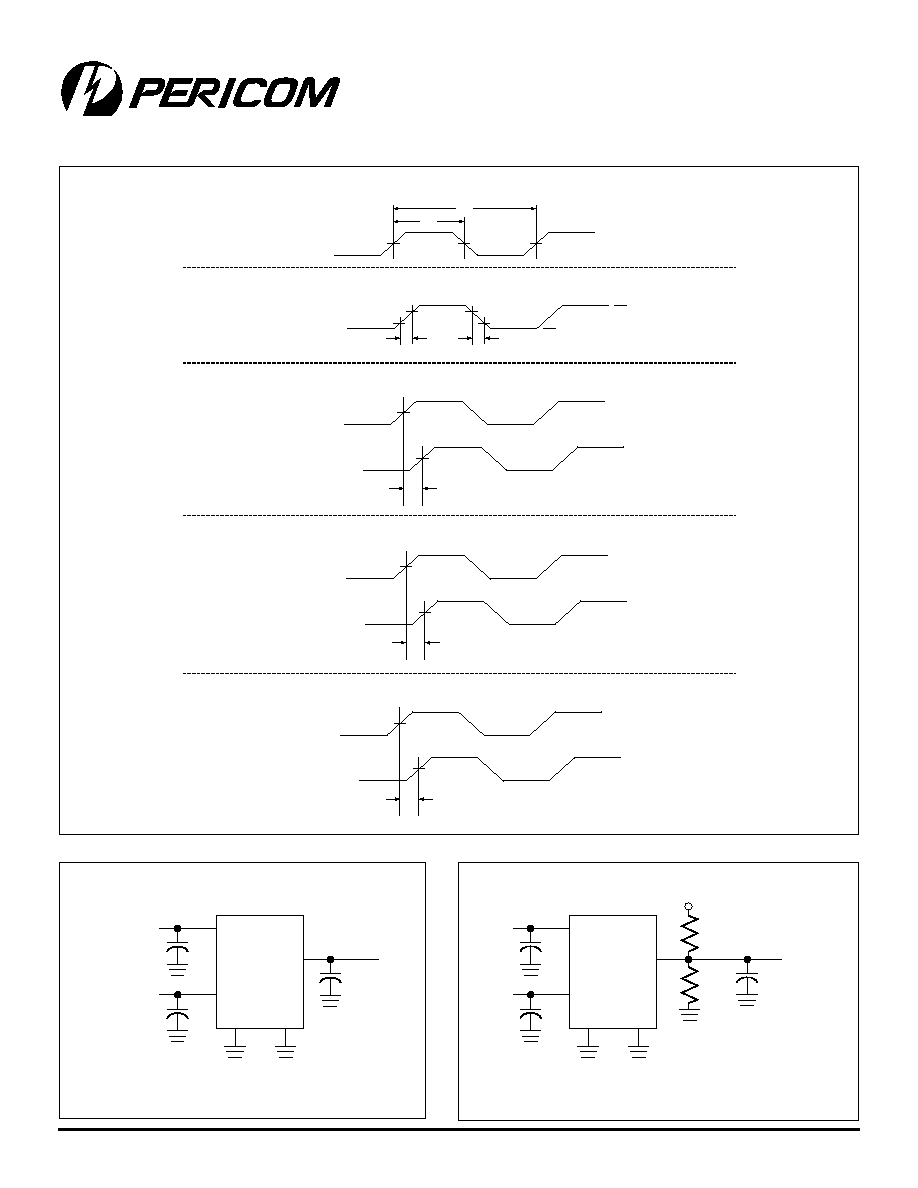
Test Circuit for all parameters except t
8
V
DD
10pF
V
DD
GND
GND
CLK out
OUTPUTS
0.1
m
F
0.1
m
F
Test Circuit for t
8
,Output slew rate on -1H device
1k
W
1k
W
Switching Waveforms
Test Circuit #2
Test Circuit #1
t
2
t
1
1.4V
1.4V
1.4V
t
4
t
3
0.8V
2.0V
0.8V
2.0V
OUTPUT
0V
3.3V
1.4V
t
5
OUTPUT
1.4V
OUTPUT
V
DD
/2
t
6
INPUT
V
DD
/2
FBK
V
DD
/2
t
7
FBK Device 1
V
DD
/2
FBK Device 2
Duty Cycle Timing
All Outputs Rise/Fall Time
Output-Output Skew
Input-Output Propagation Delay
Device-Device Skew
9
PS8384D 06/26/01
12345678901234567890123456789012123456789012345678901234567890121234567890123456789012345678901212345678901234567890123456789012123456789012
12345678901234567890123456789012123456789012345678901234567890121234567890123456789012345678901212345678901234567890123456789012123456789012
PI6C2308
3.3V Zero Delay Buffer
16-Pin SOIC (W)
Note: Controlling dimensions in millimeters. Ref: JEDEC MS - 012 AC
16-Pin TSSOP (L)
SEATING PLANE
.050
BSC
1
16
0-8∞
.149
.157
X.XX
X.XX
DENOTES DIMENSIONS
IN MILLIMETERS
3.78
3.99
.386
.393
9.80
10.00
1.27
.053
.068
1.35
1.75
.2284
.2440
5.80
6.20
.0040
.0098
0.10
0.25
.013
.020
.0155
.0260
0.330
0.508
0.393
0.660
.0075
.0098
0.25
0.50
.0099
.0196
x 45∞
0.19
0.25
.016
.050
0.41
1.27
REF
.193
.201
.047
max.
.002
.006
SEATING
PLANE
.0256
BSC
.018
.030
.004
.008
.252
BSC
1
16
.169
.177
X.XX
X.XX
DENOTES CONTROLLING
DIMENSIONS IN MILLIMETERS
0.05
0.15
6.4
0.45
0.75
0.09
0.20
4.3
4.5
1.20
4.9
5.1
0.65
0.19
0.30
.007
.012

10
PS8384D 06/26/01
12345678901234567890123456789012123456789012345678901234567890121234567890123456789012345678901212345678901234567890123456789012123456789012
12345678901234567890123456789012123456789012345678901234567890121234567890123456789012345678901212345678901234567890123456789012123456789012
PI6C2308
3.3V Zero Delay Buffer
Pericom Semiconductor Corporation
2380 Bering Drive ∑ San Jose, CA 95131 ∑ 1-800-435-2336 ∑ Fax (408) 435-1100 ∑ http://www.pericom.com
e
d
o
C
g
n
i
r
e
d
r
O
e
m
a
N
e
g
a
k
c
a
P
e
p
y
T
e
g
a
k
c
a
P
e
g
n
a
R
g
n
it
a
r
e
p
O
W
1
-
8
0
3
2
C
6
I
P
6
1
W
C
I
O
S
li
m
-
0
5
1
n
i
p
-
6
1
l
ai
c
r
e
m
m
o
C
W
H
1
-
8
0
3
2
C
6
I
P
W
2
-
8
0
3
2
C
6
I
P
W
3
-
8
0
3
2
C
6
I
P
W
4
-
8
0
3
2
C
6
I
P
W
6
-
8
0
3
2
C
6
I
P
L
1
-
8
0
3
2
C
6
I
P
6
1
L
P
O
S
S
T
n
i
p
-
6
1
L
H
1
-
8
0
3
2
C
6
I
P
Ordering Information (Commercial Temperature Device)
e
d
o
C
g
n
i
r
e
d
r
O
e
m
a
N
e
g
a
k
c
a
P
e
p
y
T
e
g
a
k
c
a
P
e
g
n
a
R
g
n
it
a
r
e
p
O
I
W
1
-
8
0
3
2
C
6
I
P
6
1
W
C
I
O
S
li
m
-
0
5
1
n
i
p
-
6
1
l
ai
rt
s
u
d
n
I
I
W
H
1
-
8
0
3
2
C
6
I
P
I
W
2
-
8
0
3
2
C
6
I
P
I
W
3
-
8
0
3
2
C
6
I
P
I
W
4
-
8
0
3
2
C
6
I
P
I
W
6
-
8
0
3
2
C
6
I
P
I
L
1
-
8
0
3
2
C
6
I
P
6
1
L
P
O
S
S
T
n
i
p
-
6
1
I
L
H
1
-
8
0
3
2
C
6
I
P
Ordering Information (Industrial Temperature Device)