PI74FCT16823T/162823/162H823T
18-BIT REGISTERS
1
PS2040A 03/11/96
12345678901234567890123456789012123456789012345678901234567890121234567890123456789012345678901212345678901234567890123456789012123456789012
12345678901234567890123456789012123456789012345678901234567890121234567890123456789012345678901212345678901234567890123456789012123456789012
12345678901234567890123456789012123456789012345678901234567890121234567890123456789012345678901212345678901234567890123456789012123456789012
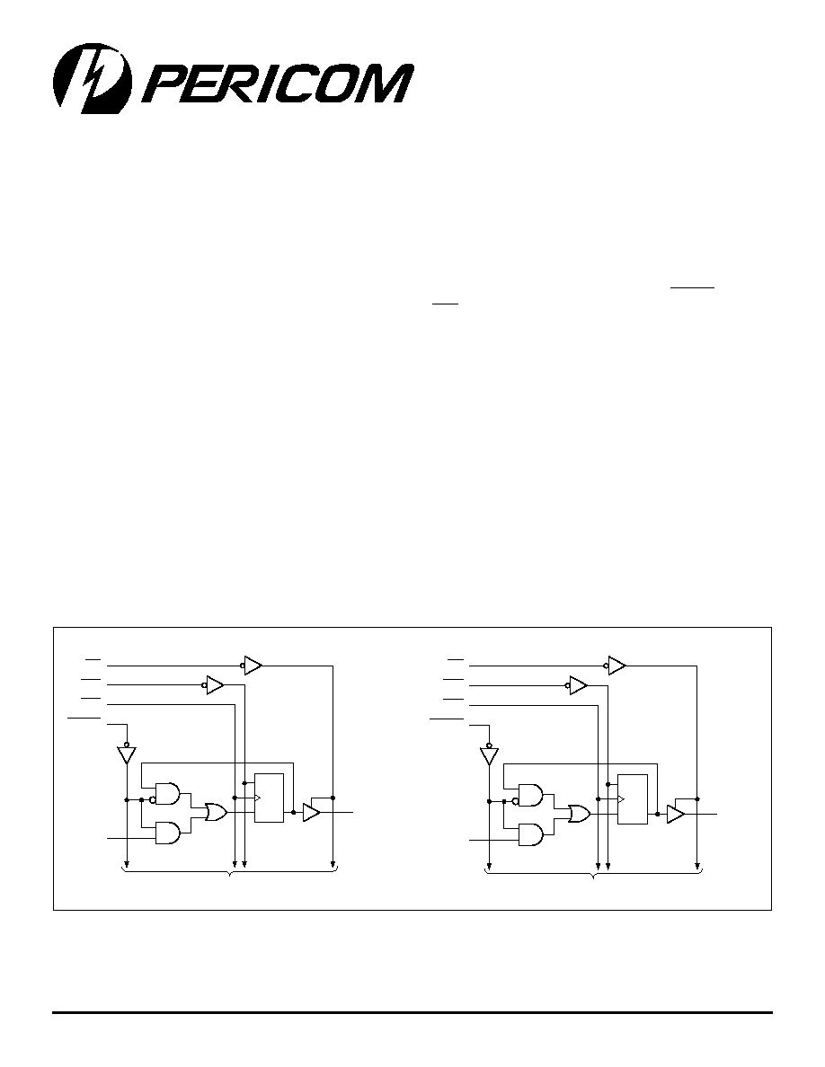
Logic Block Diagram
Product Features:
Common Features:
∑ PI74FCT16823T and PI74FCT162823T are high-speed, low
power devices with high current drive.
∑ V
CC
= 5V ±10%
∑ Hysteresis on all inputs
∑ Packages available:
≠ 56-pin 240 mil wide plastic TSSOP (A)
≠ 56-pin 300 mil wide palstic SSOP (V)
PI74FCT16823T Features:
∑ High output drive: I
OH
= ≠32 mA; I
OL
= 64 mA
∑ Power off disable outputs permit "live insertion"
∑ Typical V
OLP
(Output Ground Bounce) < 1.0V
at V
CC
= 5V, T
A
= 25∞C
PI74FCT162823T Features:
∑ Balanced output drivers: ±24 mA
∑ Reduced system switching noise
∑ Typical V
OLP
(Output Ground Bounce) < 0.6V
at V
CC
= 5V, T
A
= 25∞C
PI74FCT162H823T Features:
∑ Bus Hold retains last active bus state during 3-state
∑ Eliminates the need for external pull-up resistors
PI74FCT16823T
PI74FCT162823T
PI74FCT162H823T
Fast CMOS
18-Bit Registers
Product Description:
Pericom Semiconductor's PI74FCT series of logic circuits are pro-
duced in the Company's advanced 0.6 micron CMOS technology,
achieving industry leading speed grades.
The PI74FCT16823T, PI74FCT162823T and PI74FCT162H823
are 18-bit wide registers with clock enable (xCLKEN) and clear
(xCLR) controls that make these devices especially suitable for
parity bus interfacing in high-performance systems. The devices
can be operated as two 9-bit registers or one 18-bit register using the
control inputs. Signal pins are arranged in a flow-through
organization for ease of layout and hysteresis is designed into all
inputs to improve noise margin.
The PI74FCT16823T output buffers are designed with a Power-
Off disable function allowing "live insertion" of boards when the
devices are used as backplane drives.
The PI74FCT162823T has ±24 mA balanced output drivers. It is
designed with current limiting resistors at its outputs to control the
output edge rate resulting in lower ground bounce and undershoot.
This eliminates the need for external terminating resistors for most
interface applications.
The PI74FCT162H823T has "Bus Hold" which retains the input's
last state whenever the input goes to high-impedance preventing
"floating" inputs and eliminating the need for pull-up/down resistors.
R
C
1
OE
D
1
CLR
1
CLK
1
CLKEN
1
D
1
1
Q
1
To 8 other channels
R
C
2
OE
D
2
CLR
2
CLK
2
CLKEN
2
D
1
2
Q
1
To 8 other channels

PI74FCT16823T/162823/162H823T
18-BIT REGISTERS
2
PS2040A 03/11/96
12345678901234567890123456789012123456789012345678901234567890121234567890123456789012345678901212345678901234567890123456789012123456789012
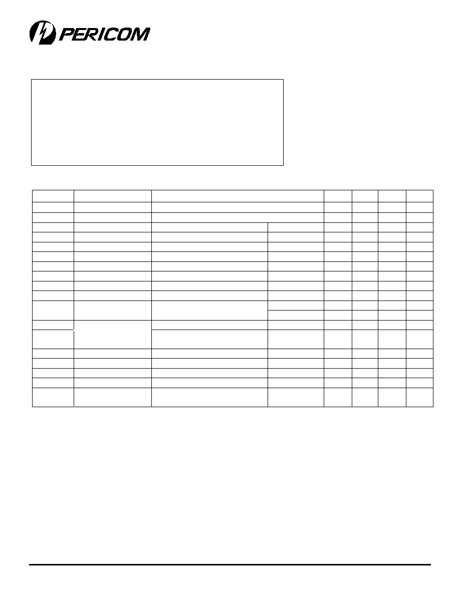
Pin Name
Description
xDx
Data Inputs
(1)
xCLK
Clock Inputs
xCLKEN
Clock Enable Inputs (Active LOW)
xCLR
Asynchronous Clear Inputs (Active LOW)
xOE
Output Enable Inputs (Active LOW)
xQx
3-State Outputs
Note:
1. For the PI74FCT162H823T, these pins have "Bus
Hold." All other pins are standard, outputs, or I/Os.
Product Pin Description
Product Pin Configuration
PI74FCT16823 Truth Table
(1)
Inputs
Outputs
Function
xOE
xCLR xCLKEN xCLK
xDx
xQx
High-Z
H
X
X
X
X
Z
Clear
L
L
X
X
X
L
Hold
L
H
H
X
X
Q
(2)
Load
H
H
L
L
Z
H
H
L
H
Z
L
H
L
L
L
L
H
L
H
H
1.
H = High Voltage Level
L = Low Voltage Level
X = Don't Care
Z = High Impedance
NC = No Change
=
LOW-to-HIGH Transition
2.
Output level before indicated steady-state
input conditions were established.
1
CLR
1
1
OE
2
1
Q
1
3
GND
4
1
Q
2
5
1
Q
3
6
V
CC
7
1
Q
4
8
1
Q
5
9
1
Q
6
10
GND
11
1
Q
7
12
1
Q
8
13
1
Q
9
14
2
Q
1
15
2
Q
2
16
2
Q
3
17
GND
18
2
Q
4
19
2
Q
5
20
2
Q
6
21
V
CC
22
2
Q
7
23
2
Q
8
24
1
CLK
56
1
CLKEN
55
1
D
1
54
GND
53
1
D
2
52
1
D
3
51
V
CC
50
1
D
4
49
1
D
5
48
1
D
6
47
GND
46
1
D
7
45
1
D
8
44
1
D
9
43
2
D
1
42
2
D
2
41
2
D
3
40
GND
39
2
D
4
38
2
D
5
37
2
D
6
36
V
CC
35
2
D
7
34
2
D
8
33
GND
25
2
Q
9
26
2
OE
27
2
CLR
28
GND
32
2
D
9
31
2
CLKEN
30
2
CLK
29
56-PIN
V56
A56
PI74FCT16823T/162823/162H823T
18-BIT REGISTERS
3
PS2040A 03/11/96
12345678901234567890123456789012123456789012345678901234567890121234567890123456789012345678901212345678901234567890123456789012123456789012
DC Electrical Characteristics
(Over the Operating Range, T
A
= ≠40∞C to +85∞C, V
CC
= 5.0V ± 10%)
Parameters Description
Test Conditions
(1)
Min.
Typ
(2)
Max.
Units
V
IH
Input HIGH Voltage
Guaranteed Logic HIGH Level
2.0
V
V
IL
Input LOW Voltage
Guaranteed Logic LOW Level
0.8
V
I
IH
Input HIGH Current
Standard Input, V
CC
= Max.
V
IN
= V
CC
1
µA
I
IH
Input HIGH Current
Standard I/O, V
CC
= Max.
V
IN
= V
CC
1
µA
I
IH
Input HIGH Current
Bus Hold Input
(4)
, V
CC
= Max.
V
IN
= V
CC
±100
µA
I
IH
Input HIGH Current
Bus Hold I/O
(4)
, V
CC
= Max.
V
IN
= V
CC
±100
µA
I
IL
Input LOW Current
Standard Input, V
CC
= Min.
V
IN
= GND
≠1
µA
I
IL
Input LOW Current
Standard I/O, V
CC
= Min.
V
IN
= GND
≠1
µA
I
IL
Input LOW Current
Bus Hold Input
(4)
, V
CC
= Min.
V
IN
= GND
±100
µA
I
IL
Input LOW Current
Bus Hold I/O
(4)
, V
CC
= Min.
V
IN
= GND
±100
µA
I
BHH
Bus Hold
Bus Hold Input
(4)
, V
CC
= Min.
V
IN
= 2.0V
≠50
µA
I
BHL
Sustain Current
V
IN
= 0.8V
+50
I
OZH
(5)
High-Impedance
V
CC
= Max.
V
OUT
= 2.7V
1
µA
I
OZL
(5)
Output Current
V
CC
= Max.
V
OUT
= 0.5V
≠1
µA
(3-S
TATE
O
UTPUTS
)
V
IK
Clamp Diode Voltage
V
CC
= Min., I
IN
= ≠18 mA
≠0.7
≠1.2
V
I
OS
Short Circuit Current
V
CC
= Max.
(3)
, V
OUT
= GND
≠80
≠140
≠200
mA
I
O
Output Drive Current
V
CC
= Max.
(3)
, V
OUT
= 2.5V
≠50
≠180
mA
V
H
Input Hysteresis
100
mV
Maximum Ratings
(Above which the useful life may be impaired. For user guidelines, not tested.)
Storage Temperature .................................................................... ≠65∞C to +150∞C
Ambient Temperature with Power Applied .................................... ≠40∞C to +85∞C
Supply Voltage to Ground Potential (Inputs & Vcc Only) .............. ≠0.5V to +7.0V
Supply Voltage to Ground Potential (Outputs & D/O Only) ........... ≠0.5V to +7.0V
DC Input Voltage ............................................................................ ≠0.5V to +7.0V
DC Output Current ..................................................................................... 120 mA
Power Dissipation .......................................................................................... 1.0W
Note:
Stresses greater than those listed under
MAXIMUM RATINGS may cause permanent
damage to the device. This is a stress rating
only and functional operation of the device at
these or any other conditions above those
indicated in the operational sections of this
specification is not implied. Exposure to
absolute maximum rating conditions for
extended periods may affect reliability.
Notes:
1. For Max. or Min. conditions, use appropriate value specified under Electrical Characteristics for the applicable device type.
2. Typical values are at Vcc = 5.0V, +25∞C ambient and maximum loading.
3. Not more than one output should be shorted at one time. Duration of the test should not exceed one second.
4. Pins with Bus Hold are identified in the pin description.
5. This specification does not apply to bi-directional functionalities with Bus Hold.

PI74FCT16823T/162823/162H823T
18-BIT REGISTERS
4
PS2040A 03/11/96
12345678901234567890123456789012123456789012345678901234567890121234567890123456789012345678901212345678901234567890123456789012123456789012
PI74FCT16823T Output Drive Characteristics
(Over the Operating Range)
Parameters Description
Test Conditions
(1)
Min.
Typ
(2)
Max.
Units
V
OH
Output HIGH Voltage
V
CC
= Min., V
IN
= V
IH
or V
IL
I
OH
= ≠3.0 mA
2.5
3.5
V
I
OH
= ≠15.0 mA
2.4
3.5
I
OH
= ≠32.0 mA
2.0
3.0
V
OL
Output LOW Voltage
V
CC
= Min., V
IN
= V
IH
or V
IL
I
OL
= 64 mA
0.2
0.55
V
I
OFF
Power Down Disable
V
CC
= 0V, V
IN
or V
OUT
4.5V
--
--
±100
µA
PI74FCT162823T/162H823T Output Drive Characteristics
(Over the Operating Range)
Parameters Description
Test Conditions
(1)
Min.
Typ
(2)
Max.
Units
V
OH
Output HIGH Voltage
V
CC
= Min., V
IN
= V
IH
or V
IL
I
OH
= ≠24.0 mA
2.4
3.3
V
V
OL
Output LOW Voltage
V
CC
= Min., V
IN
= V
IH
or V
IL
I
OL
= 24 mA
0.3
0.55
V
I
ODL
Output LOW Current
V
CC
= 5V, V
IN
= V
IH
OR
V
IL
, V
OUT
= 1.5V
(3)
60
115
150
mA
I
ODH
Output HIGH Current
V
CC
= 5V, V
IN
= V
IH
OR
V
IL
, V
OUT
= 1.5V
(3)
≠60
≠115
≠150
mA
Notes:
1. For Max. or Min. conditions, use appropriate value specified under Electrical Characteristics for the applicable device type.
2. Typical values are at Vcc = 5.0V, +25∞C ambient and maximum loading.
3. Not more than one output should be shorted at one time. Duration of the test should not exceed one second.
4. This parameter is determined by device characterization but is not production tested.
Capacitance
(T
A
= 25∞C, f = 1 MHz)
Parameters
(4)
Description
Test Conditions
Typ
Max.
Units
C
IN
Input Capacitance
V
IN
= 0V
4.5
6
pF
C
OUT
Output Capacitance
V
OUT
= 0V
5.5
8
pF

PI74FCT16823T/162823/162H823T
18-BIT REGISTERS
5
PS2040A 03/11/96
12345678901234567890123456789012123456789012345678901234567890121234567890123456789012345678901212345678901234567890123456789012123456789012
Notes:
1. For conditions shown as Max. or Min., use appropriate value specified under Electrical Characteristics for the applicable device.
2. Typical values are at Vcc = 5.0V, +25∞C ambient.
3. Per TTL driven input (V
IN
= 3.4V); all other inputs at Vcc or GND.
4. This parameter is not directly testable, but is derived for use in Total Power Supply Calculations.
5. Values for these conditions are examples of the Icc formula. These limits are guaranteed but not tested.
6. I
C
=I
QUIESCENT
+ I
INPUTS
+ I
DYNAMIC
I
C
= I
CC
+
I
CC
D
H
N
T
+ I
CCD
(f
CP
/2 + f
I
N
I
)
I
CC
= Quiescent Current
I
CC
= Power Supply Current for a TTL High Input (V
IN
= 3.4V).
D
H
= Duty Cycle for TTL Inputs High.
N
T
= Number of TTL Inputs at D
H
.
I
CCD
= Dynamic Current Caused by an Input Transition Pair (HLH or LHL).
f
CP
= Clock Frequency for Register Devices (Zero for Non-Register Devices)
f
I
= Input Frequency
N
I
= Number of Inputs at f .
All currents are in milliamps and all frequencies are in megahertz.
Power Supply Characteristics
Parameters Description
Test Conditions
(1)
Min.
Typ
(2)
Max.
Units
I
CC
Quiescent Power
V
CC
= Max.
V
IN
= GND
0.1
500
µA
Supply Current
or V
CC
I
CC
Supply Current per
V
CC
= Max.
V
IN
= 3.4V
(3)
0.5
1.5
mA
Input @ TTL HIGH
I
CCD
Supply Current per
V
CC
= Max.,
V
IN
= V
CC
75
120
µA/
Input per MHz
(4)
Outputs Open
V
IN
= GND
MHz
X
OE = xCLKEN = GND
One Input Toggling
50% Duty Cycle
I
C
Total Power Supply
V
CC
= Max.,
V
IN
= V
CC
0.8
2.7
mA
Current
(6)
Outputs Open
V
IN
= GND
f
CP
= 10 MH
Z
50% Duty Cycle
V
IN
= 3.4V
1.3
3.2
X
OE = xCLKEN = GND
V
IN
= GND
f
I
= 5 MH
Z
One Bit Toggling
V
CC
= Max.,
V
IN
= V
CC
4.2
7.1
(5)
Outputs Open
V
IN
= GND
f
CP
= 10 MH
Z
50% Duty Cycle
V
IN
= 3.4V
9.2
22.1
(5)
X
OE = xCLKEN = GND
V
IN
= GND
Eighteen Bits Toggling
f
I
= 2.5 MH
Z
50% Duty Cycle

PI74FCT16823T/162823/162H823T
18-BIT REGISTERS
6
PS2040A 03/11/96
12345678901234567890123456789012123456789012345678901234567890121234567890123456789012345678901212345678901234567890123456789012123456789012
PI74FCT16823T Switching Characteristics over Operating Range
16823AT
16823BT
16823CT
16823DT
16823ET
Com.
Com.
Com.
Com.
Com.
Parameters
Description
Conditions
(1)
Min
Max
Min
Max
Min
Max
Min
Max
Min
Max
Unit
t
PLH
Propagation Delay
C
L
= 50 pF
1.5
10.0
1.5
7.5
1.5
6.0
1.5
5.0
1.5
4.4
ns
t
PHL
X
CLK to
X
Q
X
R
L
= 500
C
L
= 300 pF
(3)
1.5
20.0
1.5
15.0
1.5
12.5
1.5
8.5
1.5
8.0
ns
R
L
= 500
t
PHL
Propagation Delay
C
L
= 50 pF
1.5
14.0
1.5
9.0
1.5
8.0
1.5
5.0
1.5
4.4
ns
X
CLR to
X
Q
X
R
L
= 500
t
PZH
Output Enable Time
C
L
= 50 pF
1.5
12.0
1.5
8.0
1.5
7.0
1.5
4.8
1.5
4.4
ns
t
PZL
X
OE to
X
Q
X
R
L
= 500
C
L
= 300 pF
(3)
1.5
23.0
1.5
15.0
1.5
12.5
1.5
10.0
1.5
9.0
ns
R
L
= 500
t
PHZ
Output Disable Time
(3)
C
L
= 5 pF
(3)
1.5
7.0
1.5
6.5
1.5
6.2
1.5
5.0
1.5
4.0
ns
t
PLZ
X
OE to
X
Q
X
R
L
= 500
C
L
= 50 pF
1.5
8.0
1.5
7.5
1.5
6.5
1.5
5.0
1.5
4.0
ns
R
L
= 500
t
SU
Setup Time HIGH or
C
L
= 50 pF
4.0
--
3.0
--
3.0
--
3.0
--
1.5
--
ns
LOW,
X
D
X
to
X
CLK
R
L
= 500
t
H
Hold Time HIGH or
2.0
--
1.5
--
1.5
--
1.5
--
0
--
ns
LOW,
X
D
X
to
X
CLK
t
SU
Setup Time HIGH or
4.0
--
3.0
--
3.0
--
3.0
--
2.5
--
ns
LOW,
X
CLKEN to
X
CLK
t
H
Hold Time HIGH or
2.0
--
0
--
0
--
0
--
0
--
ns
LOW,
X
CLKEN to
X
CLK
t
W
xCLK Pulse Width
7.0
--
6.0
--
6.0
--
6.0
--
3.0
--
ns
HIGH or LOW
(3)
t
W
xCLR Pulse Width LOW
(3)
6.0
--
6.0
--
6.0
--
6.0
--
3.0
--
ns
t
REM
Recovery Time
(3)
6.0
--
6.0
--
6.0
--
6.0
--
3.0
--
ns
X
CLR to
X
CLK
t
SK
(
O
)
Output Skew
(4)
--
0.5
--
0.5
--
0.5
--
0.5
--
0.5
ns
Notes:
1. See test circuit and wave forms.
2. Minimum limits are guaranteed but not tested on Propagation Delays.
3. This parameter is guaranteed but not production tested.
4. Skew between any two outputs, of the same package, switching in the same direction. This parameter is guaranteed by design.

PI74FCT16823T/162823/162H823T
18-BIT REGISTERS
7
PS2040A 03/11/96
12345678901234567890123456789012123456789012345678901234567890121234567890123456789012345678901212345678901234567890123456789012123456789012
PI74FCT162823T Switching Characteristics over Operating Range
162823AT
162823BT
162823CT
162823DT
162823ET
Com.
Com.
Com.
Com.
Com.
Parameters
Description
Conditions
(1)
Min
Max
Min
Max
Min
Max
Min
Max
Min
Max
Unit
t
PLH
Propagation Delay
C
L
= 50 pF
1.5
10.0
1.5
7.5
1.5
6.0
1.5
5.0
1.5
4.4
ns
t
PHL
X
CLK to
X
Q
X
R
L
= 500
C
L
= 300 pF
(3)
1.5
20.0
1.5
15.0
1.5
12.5
1.5
8.5
1.5
8.0
ns
R
L
= 500
t
PHL
Propagation Delay
C
L
= 50 pF
1.5
14.0
1.5
9.0
1.5
8.0
1.5
5.0
1.5
4.4
ns
X
CLR to
X
Q
X
R
L
= 500
t
PZH
Output Enable Time
C
L
= 50 pF
1.5
12.0
1.5
8.0
1.5
7.0
1.5
4.8
1.5
4.4
ns
t
PZL
X
OE to
X
Q
X
R
L
= 500
C
L
= 300 pF
(3)
1.5
23.0
1.5
15.0
1.5
12.5
1.5
10.0
1.5
9.0
ns
R
L
= 500
t
PHZ
Output Disable Time
(3)
C
L
= 5 pF
(3)
1.5
7.0
1.5
6.5
1.5
6.2
1.5
5.0
1.5
4.0
ns
t
PLZ
X
OE to
X
Q
X
R
L
= 500
C
L
= 50 pF
1.5
8.0
1.5
7.5
1.5
6.5
1.5
5.0
1.5
4.0
ns
R
L
= 500
t
SU
Setup Time HIGH or
C
L
= 50 pF
4.0
--
3.0
--
3.0
--
3.0
--
1.5
--
ns
LOW,
X
D
X
to
X
CLK
R
L
= 500
t
H
Hold Time HIGH or
2.0
--
1.5
--
1.5
--
1.5
--
0
--
ns
LOW,
X
D
X
to
X
CLK
t
SU
Setup Time HIGH or
4.0
--
3.0
--
3.0
--
3.0
--
2.5
--
ns
LOW,
X
CLKEN to
X
CLK
t
H
Hold Time HIGH or
2.0
--
0
--
0
--
0
--
0
--
ns
LOW,
X
CLKEN to
X
CLK
t
W
xCLK Pulse Width
7.0
--
6.0
--
6.0
--
6.0
--
3.0
--
ns
HIGH or LOW
(3)
t
W
xCLR Pulse Width LOW
(3)
6.0
--
6.0
--
6.0
--
6.0
--
3.0
--
ns
t
REM
Recovery Time
(3)
6.0
--
6.0
--
6.0
--
6.0
--
3.0
--
ns
X
CLR to
X
CLK
t
SK
(
O
)
Output Skew
(4)
--
0.5
--
0.5
--
0.5
--
0.5
--
0.5
ns
Notes:
1. See test circuit and wave forms.
2. Minimum limits are guaranteed but not tested on Propagation Delays.
3. This parameter is guaranteed but not production tested.
4. Skew between any two outputs, of the same package, switching in the same direction. This parameter is guaranteed by design.
PI74FCT16823T/162823/162H823T
18-BIT REGISTERS
8
PS2040A 03/11/96
12345678901234567890123456789012123456789012345678901234567890121234567890123456789012345678901212345678901234567890123456789012123456789012
PI74FCT162H823T Switching Characteristics over Operating Range
162H823AT
162H823BT
1628H23CT
162H823DT
162H823ET
C o m .
C o m .
C o m .
C o m .
C o m .
Parameters
Description
Conditions
(1)
Min
Max
Min
Max
Min
Max
Min
Max
Min
Max
Unit
t
PLH
Propagation Delay
C
L
= 50 pF
1.5
10.0
1.5
7.5
1.5
6.0
1.5
5.0
1.5
4.4
ns
t
PHL
X
CLK to
X
Q
X
R
L
= 500
C
L
= 300 pF
(3)
1.5
20.0
1.5
15.0
1.5
12.5
1.5
8.5
1.5
8.0
ns
R
L
= 500
t
PHL
Propagation Delay
C
L
= 50 pF
1.5
14.0
1.5
9.0
1.5
8.0
1.5
5.0
1.5
4.4
ns
X
CLR to
X
Q
X
R
L
= 500
t
PZH
Output Enable Time
C
L
= 50 pF
1.5
12.0
1.5
8.0
1.5
7.0
1.5
4.8
1.5
4.4
ns
t
PZL
X
OE to
X
Q
X
R
L
= 500
C
L
= 300 pF
(3)
1.5
23.0
1.5
15.0
1.5
12.5
1.5
10.0
1.5
9.0
ns
R
L
= 500
t
PHZ
Output Disable Time
(3)
C
L
= 5 pF
(3)
1.5
7.0
1.5
6.5
1.5
6.2
1.5
5.0
1.5
4.0
ns
t
PLZ
X
OE to
X
Q
X
R
L
= 500
C
L
= 50 pF
1.5
8.0
1.5
7.5
1.5
6.5
1.5
5.0
1.5
4.0
ns
R
L
= 500
t
SU
Setup Time HIGH or
C
L
= 50 pF
4.0
--
3.0
--
3.0
--
3.0
--
1.5
--
ns
LOW,
X
D
X
to
X
CLK
R
L
= 500
t
H
Hold Time HIGH or
2.0
--
1.5
--
1.5
--
1.5
--
0
--
ns
LOW,
X
D
X
to
X
CLK
t
SU
Setup Time HIGH or
4.0
--
3.0
--
3.0
--
3.0
--
2.5
--
ns
LOW,
X
CLKEN to
X
CLK
t
H
Hold Time HIGH or
2.0
--
0
--
0
--
0
--
0
--
ns
LOW,
X
CLKEN to
X
CLK
t
W
xCLK Pulse Width
7.0
--
6.0
--
6.0
--
6.0
--
3.0
--
ns
HIGH or LOW
(3)
t
W
xCLR Pulse Width LOW
(3)
6.0
--
6.0
--
6.0
--
6.0
--
3.0
--
ns
t
REM
Recovery Time
(3)
6.0
--
6.0
--
6.0
--
6.0
--
3.0
--
ns
X
CLR to
X
CLK
t
SK
(
O
)
Output Skew
(4)
--
0.5
--
0.5
--
0.5
--
0.5
--
0.5
ns
Notes:
1. See test circuit and wave forms.
2. Minimum limits are guaranteed but not tested on Propagation Delays.
3. This parameter is guaranteed but not production tested.
4. Skew between any two outputs, of the same package, switching in the same direction. This parameter is guaranteed by design.
Pericom Semiconductor Corporation
2380 Bering Drive ∑ San Jose, CA 95131 ∑ 1-800-435-2336 ∑ Fax (408) 435-1100 ∑ http://www.pericom.com