
PI74FCT163373
3.3V 16-BIT TRANSPARENT LATCH
12345678901234567890123456789012123456789012345678901234567890121234567890123456789012345678901212345678901234567890123456789012123456789012
1
PS2055B 01/18/99
12345678901234567890123456789012123456789012345678901234567890121234567890123456789012345678901212345678901234567890123456789012123456789012
12345678901234567890123456789012123456789012345678901234567890121234567890123456789012345678901212345678901234567890123456789012123456789012
PI74FCT163373
Fast CMOS 3.3V 16-Bit
Transparent Latch
Product Description
Pericom Semiconductor's PI74FCT series of logic circuits are
produced in the Company's advanced 0.6 micron CMOS
technology, achieving industry leading speed grades.
The PI74FCT163373 is a 16-bit transparent latch designed with
3-state outputs and are intended for bus oriented applications. The
Output Enable and Latch Enable controls are organized to operate
as two 8-bit latches or one 16-bit latch. When Latch Enable (LE)
is HIGH, the flip-flops appear transparent to the data. The data that
meets the set-up time when LE is LOW is latched. When OE is
HIGH, the bus output is in the high impedance state.
Product Features
∑ Advanced Low Power CMOS Operation
∑ Can serve as a 5V to 3V translator
∑ Excellent output drive capability:
Balanced drives (24mA sink and source)
Compatible with LVC
TM
class of products.
∑ Pin compatible with industry standard
double-density pinouts
∑ Low ground bounce outputs
∑ Hysteresis on all inputs
∑ Industrial operating temperature range: ≠40∞C to +85∞C
∑ Inputs can be driven by 3.3V or 5V devices
∑ Multiple center pin and distributed Vcc/GND pins
minimizing switching noise
∑ Packages available:
≠ 48-pin 240 mil wide plastic TSSOP (A)
≠ 48-pin 300 mil wide plastic SSOP (V)
≠ 48-pin 173 mil wide plastic TVSOP (K)
∑ Device models available on request
Logic Block Diagram
1
OE
1
LE
1
O
0
C
D
1
D
0
TO 7 OTHER CHANNELS
2
OE
2
LE
2
O
0
C
D
2
D
0
TO 7 OTHER CHANNELS
PI74FCT163373
3.3V 16-BIT TRANSPARENT LATCH
2
PS2055B 01/18/99
12345678901234567890123456789012123456789012345678901234567890121234567890123456789012345678901212345678901234567890123456789012123456789012
1
OE
1
1
O
0
2
1
O
1
3
GND
4
1
O
2
5
1
O
3
6
V
CC
7
1
O
4
8
1
O
5
9
GND
10
1
O
6
11
1
O
7
12
2
O
0
13
2
O
1
14
GND
15
2
O
2
16
2
O
3
17
V
CC
18
2
O
4
19
2
O
5
20
GND
21
2
O
6
22
2
O
7
23
2
OE
24
1
LE
48
1
D
0
47
1
D
1
46
GND
45
1
D
2
44
1
D
3
43
V
CC
42
1
D
4
41
1
D
5
40
GND
39
1
D
6
38
1
D
7
37
2
D
0
36
2
D
1
35
GND
34
2
D
2
33
2
D
3
32
V
CC
31
2
D
4
30
2
D
5
29
GND
28
2
D
6
27
2
D
7
26
2
LE
25
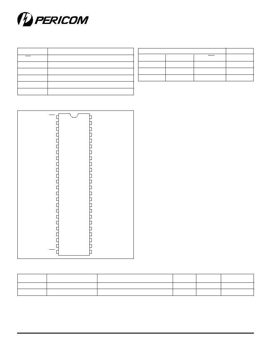
Product Pin Configuration
Product Pin Description
Pin Name
Description
xOE
3-State Output Enable Inputs (Active LOW)
xLE
Latch Enable Inputs (Active HIGH)
xDx
Data Inputs
xOx
3-State Outputs
GND
Ground
V
CC
Power
Inputs
(1)
Outputs
(1)
xDx
xLE
xOE
xOx
H
H
L
H
L
H
L
L
X
X
H
Z
Truth Table
Note:
1. H = High Voltage Level, X = Don't Care,
L = Low Voltage Level, Z = High Impedance
48-PIN
V48
A48
K48
Note:
1. This parameter is determined by device characterization but is not production tested.
Capacitance
(T
A
= 25∞C, f = 1 MHz)
Parameters
(1)
Description
Test Conditions
Typ.
Max.
Units
C
IN
Input Capacitance
V
IN
= 0V
4.5
6
pF
C
OUT
Output Capacitance
V
OUT
= 0V
5.5
8
pF
PI74FCT163373
3.3V 16-BIT TRANSPARENT LATCH
12345678901234567890123456789012123456789012345678901234567890121234567890123456789012345678901212345678901234567890123456789012123456789012
3
PS2055B 01/18/99
DC Electrical Characteristics
(Over the Operating Range, T
A
= ≠40∞C to +85∞C, V
CC
= 2.7V to 3.6V)
Parameters
Description
Test Conditions
(1)
Min.
Typ
(2)
Max.
Units
V
IH
Input HIGH Voltage (Input pins)
Guaranteed Logic HIGH Level
2.2
--
5.5
V
Input HIGH Voltage (I/O pins)
2.0
--
Vcc+0.5
V
V
IL
Input LOW Voltage
Guaranteed Logic LOW Level
≠0.5
--
0.8
V
(Input and I/O pins)
I
IH
Input HIGH Current (Input pins)
V
CC
= Max.
V
IN
= 5.5V
--
--
±1
µA
Input HIGH Current (I/O pins)
V
CC
= Max.
V
IN
= V
CC
--
--
±1
µA
I
IL
Input LOW Current (Input pins)
V
CC
= Max.
V
IN
= GND
--
--
±1
µA
Input LOW Current (I/O pins)
V
CC
= Max.
V
IN
= GND
--
--
±1
µA
I
OZH
High Impedance Output Current
V
CC
= Max.
V
OUT
= V
CC
--
--
±1
µA
I
OZL
(3-State Output pins)
V
CC
= Max.
V
OUT
= GND
--
--
±1
µA
V
IK
Clamp Diode Voltage
V
CC
= Min., I
IN
= ≠18 mA
--
≠0.7
≠1.2
V
I
ODH
Output HIGH Current
V
CC
= 3.3V, V
IN
= V
IH
or V
IL
, V
O
= 1.5V
(3)
≠36
≠60
≠110
mA
I
ODL
Output LOW Current
V
CC
= 3.3V, V
IN
= V
IH
or V
IL
, V
O
= 1.5V
(3)
50
90
200
mA
V
OH
Output HIGH Voltage
V
CC
= Min.
I
OH
= ≠0.1mA
Vcc-0.2
--
--
V
V
IN
= V
IH
or V
IL
I
OH
= ≠3mA
2.4
3.0
--
V
V
CC
= 3.0V,
I
OH
= ≠8mA
2.4
(5)
3.0
--
V
V
IN
= V
IH
OR
V
IL
I
OH
= ≠24mA
2.0
--
--
V
V
OL
Output LOW Voltage
V
CC
= Min.
I
OL
= 0.1mA
--
--
0.2
V
V
IN
= V
IH
or V
IL
I
OL
= 16mA
--
0.2
0.4
V
I
OL
= 24mA
--
0.3
0.5
V
I
OS
Short Circuit Current
(4)
V
CC
= Max.
(3)
, V
OUT
= GND
≠60
≠85
≠240
mA
V
H
Input Hysteresis
--
150
--
mV
Storage Temperature ......................................................... ≠55∞C to +125∞C
Ambient Temperature with Power Applied ........................ ≠40∞C to +85∞C
Supply Voltage to Ground Potential (Inputs & Vcc Only) .. ≠0.5V to +7.0V
Supply Voltage to Ground Potential (Outputs & D/O Only) ≠0.5V to +7.0V
DC Input Voltage ................................................................. ≠0.5V to +7.0V
DC Output Current ........................................................................... 120 mA
Power Dissipation ................................................................................. 1.0W
Note:
Stresses greater than those listed under MAXIMUM
RATINGS may cause permanent damage to the de-
vice. This is a stress rating only and functional opera-
tion of the device at these or any other conditions
above those indicated in the operational sections of
this specification is not implied. Exposure to absolute
maximum rating conditions for extended periods may
affect reliability.
Notes:
1. For Max. or Min. conditions, use appropriate value specified under Electrical Characteristics for the applicable device type.
2. Typical values are at Vcc = 3.3V, +25∞C ambient and maximum loading.
3. Not more than one output should be shorted at one time. Duration of the test should not exceed one second.
4. This parameter is guaranteed but not tested.
5. V
OH
= V
CC
≠ 0.6V at rated current.
Maximum Ratings
(Above which the useful life may be impaired. For user guidelines, not tested.)
PI74FCT163373
3.3V 16-BIT TRANSPARENT LATCH
4
PS2055B 01/18/99
12345678901234567890123456789012123456789012345678901234567890121234567890123456789012345678901212345678901234567890123456789012123456789012
Power Supply Characteristics
Parameters Description
Test Conditions
(1)
Min.
Typ
(2)
Max.
Units
I
CC
Quiescent Power Supply Current
V
CC
= Max.
V
IN
= GND or V
CC
0.1
10
µA
I
CC
Quiescent Power Supply Current
V
CC
= Max.
V
IN
= V
CC
≠ 0.6V
(3)
2.0
30
µA
TTL Inputs HIGH
I
CCD
Dynamic Power Supply
(4)
V
CC
= Max.,
V
IN
= V
CC
50
75
µA/
Outputs Open
V
IN
= GND
MHz
X
OE = GND
xLE = Vcc
One Bit Toggling
50% Duty Cycle
I
C
Total Power Supply
V
CC
= Max.,
V
IN
= V
CC
≠ 0.6V
0.5
0.8
mA
Current
(6)
Outputs Open
V
IN
= GND
f
I
= 10 MH
Z
50% Duty Cycle
X
OE = GND
X
LE = V
CC
One Bit Toggling
V
CC
= Max.,
V
IN
= V
CC
≠ 0.6V
2.0
3.3
(5)
Outputs Open
V
IN
= GND
f
I
= 2.5 MH
Z
50% Duty Cycle
X
OE = GND
X
LE = V
CC
16 Bits Toggling
Notes:
1. For Max. or Min.conditions, use appropriate value specified under Electrical Characteristics for the applicable device.
2. Typical values are at Vcc = 3.3V, +25∞C ambient.
3. Per TTL driven input; all other inputs at Vcc or GND.
4. This parameter is not directly testable, but is derived for use in Total Power Supply Calculations.
5. Values for these conditions are examples of the Icc formula. These limits are guaranteed but not tested.
6. I
C
=I
QUIESCENT
+ I
INPUTS
+ I
DYNAMIC
I
C
= I
CC
+
I
CC
D
H
N
T
+ I
CCD
(f
CP
/2 + f
I
N
I
)
I
CC
= Quiescent Current (I
CCL
, I
CCH
and I
CCZ
)
I
CC
= Power Supply Current for a TTL High Input
D
H
= Duty Cycle for TTL Inputs High
N
T
= Number of TTL Inputs at D
H
I
CCD
= Dynamic Current Caused by an Input Transition Pair (HLH or LHL)
f
CP
= Clock Frequency for Register Devices (Zero for Non-Register Devices)
N
CP
= Number of Clock Inputs at f
CP
f
I
= Input Frequency
N
I
= Number of Inputs at f
I
All currents are in milliamps and all frequencies are in megahertz.
PI74FCT163373
3.3V 16-BIT TRANSPARENT LATCH
12345678901234567890123456789012123456789012345678901234567890121234567890123456789012345678901212345678901234567890123456789012123456789012
5
PS2055B 01/18/99
Switching Characteristics over Operating Range
(1)
FCT163373
FCT163373A
FCT163373C
Com.
Com.
Com.
Parameters
Description
Conditions
(2)
Min.
(3)
Max.
Min.
(3)
Max.
Min.
(3)
Max.
Units
t
PLH
Propagation Delay
C
L
= 50 pF
1.5
8.0
1.5
5.2
1.5
4.2
ns
t
PHL
xDx to xOx
R
L
= 500
t
PLH
Propagation Delay
2.0
13.0
2.0
8.5
2.0
5.5
ns
t
PHL
xLE to xOx
t
PZH
Output Enable Time
1.5
12.0
1.5
6.5
1.5
5.5
ns
t
PZL
xOE to xOx
t
PHZ
Output Disable Time
(4)
1.5
7.5
1.5
5.5
1.5
5.0
ns
t
PLZ
xOE to xOx
t
SU
Setup Time HIGH
2.0
2.0
2.0
ns
or LOW, xDx to xLE
t
H
Hold Time HIGH
1.5
1.5
1.5
ns
or LOW, xDx to xLE
t
W
xLE Pulse Width
6.0
5.0
5.0
ns
HIGH
t
SK
(o)
Output Skew
(5)
0.5
0.5
0.5
ns
Notes:
1. Propagation Delays and Enable/Disable times are with Vcc = 3.3V ±0.3V, normal range. For Vcc = 2.7V, extended range,
all Propagation Delays and Enable/Disable times should be degraded by 20%.
2. See test circuit and wave forms.
3. Minimum limits are guaranteed but not tested on Propagation Delays.
4. This parameter is guaranteed but not production tested.
5. Skew between any two outputs, of the same package, switching in the same direction. This parameter is guaranteed by design.
Pericom Semiconductor Corporation
2380 Bering Drive ∑ San Jose, CA 95131 ∑ 1-800-435-2336 ∑ Fax (408) 435-1100 ∑ http://www.pericom.com