1
PS2083B 10/08/01
12345678901234567890123456789012123456789012345678901234567890121234567890123456789012345678901212345678901234567890123456789012123456789012
12345678901234567890123456789012123456789012345678901234567890121234567890123456789012345678901212345678901234567890123456789012123456789012
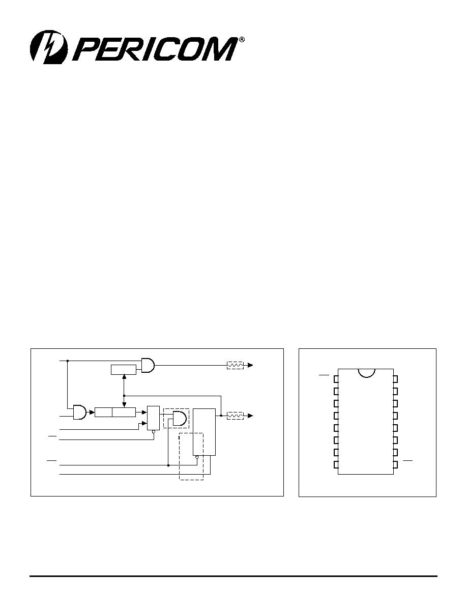
Functional Block Diagram
Product Features
∑
PI74FCT161/163/2161/2163T are pin-compatible with
bipolar FAST
TM
Series at a higher speed and lower power
consumption
∑
25
series resistor on all outputs (FCT2XXX only)
∑
TTL input and output levels
∑
Low ground bounce outputs (25
series only)
∑
Extremely low static power
∑
Hysteresis on all inputs
∑
Industrial operating temperature range: -40∞C to + 85∞C
∑
Packages available:
- 16-pin 150 mil wide plastic QSOP (Q)
- 16-pin 150 mil wide plastic SOIC (W)
- 16-pin 300 mil wide plastic SOIC (S)
Product Description
Pericom Semiconductor's PI74FCT series of logic circuits are
produced in the Company's advanced 0.6 micron CMOS technology,
achieving industry leading speed grades. All PI74FCT2XXX devices
have a built-in 25
series resistor on all outputs to reduce noise
owing to reflections, thus eliminating an external terminating
resistor.
The PI74FCT161T and PI74FCT163 are high speed CMOS
synchronous presettable 4-bit binary counters. The 161 has an
asynchronous clear, the 163 has a clocked synchronous clear. Data
is preloaded or the counters count on the rising edge of the clock.
Count enable inputs and terminal count outputs allow these counters
to be cascaded without loss of speed. Preset inputs override count
inputs, and clear inputs override both preset and count inputs. All
inputs have clamp diodes for undershoot noise suppression. All
outputs have ground bounce suppression.
PI74FCT161T/163T
(25
Series) PI74FCT2161T/2163T
High Speed CMOS Synchronous
4-Bit Binary Counters
1
V
= FF
TC
Q3-Q0
163 Only
25 Ohm
(FCT2XXX Only)
25 Ohm
(FCT2XXX Only)
161 Only
CP
MR
PE
D3-C0
CEP
CET
MUX
CLR
4-Bit
Register
Q+Cin
Cin
Pin Configurations
V
CC
MR
1
16
TC
CP
2
15
Q0
D0
3
14
Q1
D1
4
13
Q2
D2
5
12
Q3
D3
6
11
CET
CEP
7
10
PE
GND
8
9

2
PS2083B 10/08/01
12345678901234567890123456789012123456789012345678901234567890121234567890123456789012345678901212345678901234567890123456789012123456789012
12345678901234567890123456789012123456789012345678901234567890121234567890123456789012345678901212345678901234567890123456789012123456789012
PI74FCT161T/163T
(25
SERIES) PI74FCT2161T/2163T
4-BIT BINARY COUNTERS
Pin Description
Notes:
1.
H = High Voltage Level
L = Low Voltge Level
X = Don't Care
Z = High Impedance
= Low to High
e
m
a
N
n
i
P
O
/
I
n
o
i
t
p
i
r
c
s
e
D
0
D
-
3
D
I
s
t
u
p
n
I
a
t
a
D
0
Q
-
3
Q
O
s
t
u
p
t
u
O
a
t
a
D
P
C
I
k
c
o
l
C
R
M
I
t
e
s
e
R
r
e
t
s
a
M
P
E
C
I
e
l
b
a
n
E
r
e
t
n
u
o
C
T
E
C
I
e
l
b
a
n
E
C
T
d
n
a
t
n
u
o
C
C
T
O
t
n
u
o
C
l
a
n
i
m
r
e
T
E
P
I
e
l
b
a
n
E
d
a
o
L
l
e
l
l
a
r
a
P
Function Table
s
t
u
p
n
I
s
t
u
p
t
u
O
n
o
i
t
c
n
u
F
0
Q
-
3
Q
R
M
E
P
P
C
P
E
C
T
E
C
I
D
1
6
1
3
6
1
C
T
L
X
X
X
X
X
L
L
1
6
1
r
a
e
l
C
L
X
X
X
X
L
L
3
6
1
r
a
e
l
C
H
L
X
X
0
D
-
3
D
0
D
-
3
D
0
D
-
3
D
X
a
t
a
D
d
a
o
L
H
H
H
H
X
1
+
Q
1
+
Q
X
t
n
u
o
C
H
H
L
X
X
Q
Q
X
P
t
i
b
i
h
n
I
t
n
u
o
C
H
H
X
L
X
Q
Q
X
T
t
i
b
i
h
n
I
t
n
u
o
C
H
H
X
X
H
X
F
F
H
1
1
1
1
=
t
n
u
o
C
H
H
X
X
H
X
E
-
0
E
-
0
L
t
n
u
o
C
1
1
1
1
H
H
X
X
L
X
X
X
L
t
i
b
i
h
n
I
C
T
3
PS2083B 10/08/01
12345678901234567890123456789012123456789012345678901234567890121234567890123456789012345678901212345678901234567890123456789012123456789012
12345678901234567890123456789012123456789012345678901234567890121234567890123456789012345678901212345678901234567890123456789012123456789012
PI74FCT161T/163T
(25
SERIES) PI74FCT2161T/2163T
4-BIT BINARY COUNTERS
Capacitance
(T
A
= 25
∞
C, f = 1 MHz)
Notes:
1. For Max. or Min. conditions, use the appropriate values specified under Electrical Characteristics for the applicable device type.
2. Typical values are at VCC = 5.0V, +25∞C ambient and maximum loading.
3. Not more than one output should be shorted at one time. Duration of the test should not exceed one second.
4. This parameter is determined by device characterization but is not production tested.
Maximum Ratings
(Above which the useful life may be impaired. For user guidelines, not tested.)
Storage Temperature ................................................................. ≠65∞C to +150∞C
Ambient Temperature with Power Applied .................................. -40∞C to +85∞C
Supply Voltage to Ground Potential (Inputs & Vcc Only) .......... ≠0.5V to +7.0V
Supply Voltage to Ground Potential (Outputs & D/O Only) ....... ≠0.5V to +7.0V
DC Input Voltage ......................................................................... ≠0.5V to +7.0V
DC Output Current .................................................................................... 120mA
Power Dissipation ......................................................................................... 0.5W
Note:
Stresses greater than those listed under MAXIMUM
RATINGS may cause permanent damage to the
device. This is a stress rating only and functional
operation of the device at these or any other condi-
tions above those indicated in the operational sections
of this specification is not implied. Exposure to
absolute maximum rating conditions for extended
periods may affect reliability.
DC Electrical Characteristics
(Over the Operating Range, T
A
= -40∞C, Vcc = 5.0V ±5%)
s
r
e
t
e
m
a
r
a
P
n
o
i
t
p
i
r
c
s
e
D
s
n
o
i
t
i
d
n
o
C
t
s
e
T
)
1
(
.
n
i
M
p
y
T
)
2
(
.
x
a
M
s
t
i
n
U
V
OH
e
g
a
t
l
o
V
H
G
I
H
t
u
p
t
u
O
V
CC
= M
IN
,
. V
IN
= V
IH
r
o V
IL
I
OH
A
m
0
.
5
1
-
=
4
.
2
0
.
3
V
V
OL
t
n
e
r
r
u
C
W
O
L
t
u
p
t
u
O
V
CC
= M
IN
,
. V
IN
= V
IH
r
o V
IL
I
OL
A
m
8
4
=
3
.
0
0
5
.
0
V
V
OL
t
n
e
r
r
u
C
W
O
L
t
u
p
t
u
O
V
CC
= M
IN
,
. V
IN
= V
IH
r
o V
IL
I
OL
)
s
e
i
r
e
S
m
h
O
5
2
(
A
m
2
1
=
3
.
0
0
5
.
0
V
V
IH
e
g
a
t
l
o
V
H
G
I
H
t
u
p
n
I
c
i
g
o
L
d
e
e
t
n
a
r
a
u
G
H
G
I
H
l
e
v
e
L
0
.
2
V
V
IL
e
g
a
t
l
o
V
W
O
L
t
u
p
n
I
c
i
g
o
L
d
e
e
t
n
a
r
a
u
G
W
O
L
l
e
v
e
L
8
.
0
A
µ
I
IH
t
n
e
r
r
u
C
H
G
I
H
t
u
p
n
I
.
x
a
M
=
c
c
V
V
IN
V
=
CC
1
A
m
I
IL
t
n
e
r
r
u
C
W
O
L
t
u
p
n
I
.
x
a
M
=
c
c
V
V
IN
=
D
N
G
1
-
A
µ
I
OZH
e
c
n
a
d
e
p
m
I
h
g
i
H
.
x
a
M
=
c
c
V
V
OUT
=
V
7
.
2
1
A
µ
I
OZL
t
n
e
r
r
u
C
t
u
p
t
u
O
V
OUT
=
V
5
.
0
1
-
A
µ
V
IK
e
g
a
t
l
o
V
e
d
o
i
D
p
m
a
l
C
I
,
.
n
i
M
=
c
c
V
IN
A
m
8
1
-
=
7
.
0
-
2
.
1
-
A
µ
I
OFF
e
l
b
a
s
i
D
n
w
o
D
r
e
w
o
P
V
,
.
D
N
G
=
c
c
V
OUT
V
5
.
4
=
-
-
0
0
1
A
µ
I
OS
t
n
e
r
r
u
C
t
i
u
c
r
i
C
t
r
o
h
S
.
x
a
M
=
c
c
V
)
3
(
V
,
OUT
D
N
G
=
0
6
-
0
2
1
-
A
m
V
H
s
i
s
e
r
e
t
s
y
H
t
u
p
n
I
0
0
2
V
m
s
r
e
t
e
m
a
r
a
P
)
4
(
n
o
i
t
p
i
r
c
s
e
D
s
n
o
i
t
i
d
n
o
C
t
s
e
T
.
p
y
T
.
x
a
M
s
t
i
n
U
C
IN
e
c
n
a
t
i
c
a
p
a
C
t
u
p
n
I
V
IN
V
0
=
6
0
1
F
p
C
OUT
e
c
n
a
t
i
c
a
p
a
C
t
u
p
t
u
O
V
OUT
V
0
=
8
2
1
F
p

4
PS2083B 10/08/01
12345678901234567890123456789012123456789012345678901234567890121234567890123456789012345678901212345678901234567890123456789012123456789012
12345678901234567890123456789012123456789012345678901234567890121234567890123456789012345678901212345678901234567890123456789012123456789012
PI74FCT161T/163T
(25
SERIES) PI74FCT2161T/2163T
4-BIT BINARY COUNTERS
Notes:
1. For conditions shown as Max. or Min., use appropriate value specified under Electrical Characteristics for the applicable device.
2. Typical values are at Vcc = 5.0V, +25∞C ambient.
3. Per TTL driven input (V
IN
= 3.4V); all other inputs at Vcc or GND.
4. This parameter is not directly testable, but is derived for use in Total Power Supply Calculations.
5. Values for these conditions are examples of the Icc formula. These limits are guaranteed but not tested.
6. I
C
=I
QUIESCENT
+ I
INPUTS
+ I
DYNAMIC
I
C
= I
CC
+
I
CC
D
H
N
T
+ I
CCD
(f
CP
/2 + f
I
N
I
)
I
CC
= Quiescent Current
I
CC
= Power Supply Current for a TTL High Input (V
IN
= 3.4V)
D
H
= Duty Cycle for TTL Inputs High
N
T
= Number of TTL Inputs at D
H
I
CCD
= Dynamic Current Caused by an Input Transition Pair (HLH or LHL)
f
CP
= Clock Frequency for Register Devices (Zero for Non-Register Devices)
f
I
= Input Frequency
N
I
= Number of Inputs at f
I
All currents are in milliamps and all frequencies are in megahertz.
Power Supply Characteristics
s
r
e
t
e
m
a
r
a
P
n
o
i
t
p
i
r
c
s
e
D
s
n
o
i
t
i
d
n
o
C
t
s
e
T
)
1
(
.
n
i
M
p
y
T
)
2
(
.
x
a
M
s
t
i
n
U
I
C
C
r
e
w
o
P
t
n
e
c
s
e
i
u
Q
t
n
e
r
r
u
C
y
l
p
p
u
S
.
x
a
M
=
c
c
V
V
IN
V
HC
;
V
IN
V
LC
;
1
.
0
0
0
5
A
µ
D
C
C
r
e
p
t
n
e
r
r
u
C
y
l
p
p
u
S
H
G
I
H
L
T
T
@
t
u
p
n
I
x
a
M
=
c
c
V
V
IN
V
4
.
3
=
)
3
(
5
.
0
5
.
2
A
m
I
D
C
C
r
e
p
t
n
e
r
r
u
C
y
l
p
p
u
S
z
H
M
r
e
p
t
u
p
n
I
)
4
(
n
e
p
O
s
t
u
p
t
u
O
,
.
x
a
M
=
c
c
V
D
N
G
=
E
O
V
r
o
D
N
G
=
R
/
T
CC
e
l
c
y
C
y
t
u
D
%
0
5
,
g
n
i
l
g
g
o
T
t
i
B
e
n
O
V
IN
V
=
CC
;
V
IN
D
N
G
=
5
1
.
0
5
2
.
0
/
A
m
z
H
M
I
C
r
e
w
o
P
l
a
t
o
T
t
n
e
r
r
u
C
y
l
p
p
u
S
)
6
(
n
e
p
O
s
t
u
p
t
u
O
,
.
x
a
M
=
c
c
V
f
I
=
,
z
H
M
0
1
c
y
C
y
t
u
D
%
0
5
LE
=
R
/
T
E
O =
D
N
G
g
n
i
l
g
g
o
T
t
i
B
e
n
O
V
IN
V
=
CC
;
V
IN
D
N
G
=
0
.
2
0
.
4
)
5
(
A
m
V
IN
V
4
.
3
=
V
IN
D
N
G
=
3
.
2
0
.
5
)
5
(
n
e
p
O
s
t
u
p
t
u
O
,
.
x
a
M
=
c
c
V
f
I
=
,
z
H
M
0
1
e
l
c
y
C
y
t
u
D
%
0
5
=
R
/
T
E
O
D
N
G
=
t
h
g
i
E
g
n
i
l
g
g
o
T
t
i
B
V
IN
V
=
CC
;
V
IN
D
N
G
=
5
.
3
5
.
6
)
5
(
V
IN
V
4
.
3
=
V
IN
D
N
G
=
5
.
5
5
.
4
1
)
5
(

5
PS2083B 10/08/01
12345678901234567890123456789012123456789012345678901234567890121234567890123456789012345678901212345678901234567890123456789012123456789012
12345678901234567890123456789012123456789012345678901234567890121234567890123456789012345678901212345678901234567890123456789012123456789012
PI74FCT161T/163T
(25
SERIES) PI74FCT2161T/2163T
4-BIT BINARY COUNTERS
Switching Characteristics (Over Operating Range)
Notes:
1. Minimums Test Circuit and Waveforms.
2. Minimum limits are guaranteed but not tested on Propagation Delays.
3. PI74FCT2161 is available only by minimum special order.
,
T
3
6
1
,
T
1
6
1
T
3
6
1
2
,
T
1
6
1
2
,
T
A
3
6
1
,
T
A
1
6
1
T
A
3
6
1
2
,
T
A
1
6
1
2
T
C
3
6
1
,
T
C
1
6
1
l
o
b
m
y
S
n
o
i
t
p
i
r
c
s
e
D
)
1
(
s
n
o
i
t
i
d
n
o
C
.
n
i
M
.
x
a
M
.
n
i
M
.
x
a
M
.
n
i
M
.
x
a
M
s
t
i
n
U
t
Q
P
C
y
a
l
e
D
n
o
i
t
a
g
a
p
o
r
P
Q
o
t
P
C
I
)
3
/
1
6
1
(
C
L
F
p
0
5
=
R
L
m
h
O
0
0
5
=
0
.
2
5
.
9
0
.
2
2
.
6
0
.
2
6
.
5
s
n
t
Q
P
C
y
a
l
e
D
n
o
i
t
a
g
a
p
o
r
P
Q
o
t
P
C
I
)
3
/
1
6
1
2
(
C
L
F
p
0
5
=
R
L
m
h
O
0
0
5
=
0
.
2
5
.
9
0
.
2
2
.
6
s
n
t
Q
R
M
y
a
l
e
D
n
o
i
t
a
g
a
p
o
r
P
Q
o
t
R
M
I
)
1
6
1
(
C
L
F
p
0
5
=
R
L
m
h
O
0
0
5
=
0
.
2
3
1
0
.
2
5
.
8
0
.
2
8
.
7
s
n
t
Q
R
M
y
a
l
e
D
n
o
i
t
a
g
a
p
o
r
P
Q
o
t
R
M
I
)
1
6
1
2
(
C
L
F
p
0
5
=
R
L
m
h
O
0
0
5
=
0
.
2
4
1
0
.
2
1
.
9
s
n
t
C
T
P
C
y
a
l
e
D
n
o
i
t
a
g
a
p
o
r
P
C
T
o
t
P
C
C
L
F
p
0
5
=
R
L
m
h
O
0
0
5
=
0
.
2
5
1
0
.
2
8
.
9
0
.
2
8
.
8
s
n
t
C
T
E
C
y
a
l
e
D
n
o
i
t
a
g
a
p
o
r
P
C
T
o
t
T
E
C
C
L
F
p
0
5
=
R
L
m
h
O
0
0
5
=
5
.
1
5
.
8
5
.
1
5
.
5
5
.
1
0
.
5
s
n
t
C
T
R
M
y
a
l
e
D
n
o
i
t
a
g
a
p
o
r
P
C
T
o
t
R
M
C
L
F
p
0
5
=
R
L
m
h
O
0
0
5
=
5
.
1
5
.
1
1
5
.
1
5
.
7
5
.
1
8
.
6
s
n

6
PS2083B 10/08/01
12345678901234567890123456789012123456789012345678901234567890121234567890123456789012345678901212345678901234567890123456789012123456789012
12345678901234567890123456789012123456789012345678901234567890121234567890123456789012345678901212345678901234567890123456789012123456789012
PI74FCT161T/163T
(25
SERIES) PI74FCT2161T/2163T
4-BIT BINARY COUNTERS
l
o
b
m
y
S
n
o
i
t
p
i
r
c
s
e
D
s
n
o
i
t
i
d
n
o
C
,
3
6
1
,
1
6
1
,
1
6
1
2
3
6
1
2
,
A
3
6
1
,
A
1
6
1
A
1
6
1
2
A
3
6
1
2
,
,
C
3
6
1
,
C
1
6
1
C
1
6
1
2
C
3
6
1
2
,
s
t
i
n
U
n
i
M
x
a
M
n
i
M
x
a
M
n
i
M
x
a
M
t
S
e
m
i
T
p
u
t
e
S
a
t
a
D
D
I
P
C
o
t
C
L
F
p
0
5
=
R
L
m
h
O
0
0
5
=
0
.
5
0
.
4
5
.
3
s
n
t
H
e
m
i
T
d
l
o
H
a
t
a
D
D
I
P
C
o
t
5
.
1
5
.
1
5
.
1
t
H
C
e
m
i
T
p
u
t
e
S
.
b
a
n
E
t
n
u
o
C
P
C
o
t
T
E
C
,
P
E
C
5
.
1
1
5
.
9
5
.
8
t
H
e
m
i
T
d
l
o
H
e
l
b
a
n
E
t
n
u
o
C
P
C
o
t
T
E
C
,
P
E
C
0
0
0
t
S
R
M
t
S
E
P
e
m
i
T
p
u
t
e
S
l
o
r
t
n
o
C
P
C
o
t
E
P
,
R
M
5
.
1
1
5
.
9
5
.
8
t
H
R
M
t
H
E
P
e
m
i
T
d
l
o
H
l
o
r
t
n
o
C
P
C
o
t
E
P
,
R
M
5
.
1
5
.
1
5
.
1
t
W
P
C
h
t
d
i
W
e
s
l
u
P
k
c
o
l
C
)
1
(
W
O
L
r
o
H
G
I
H
0
.
5
0
.
4
0
.
3
t
W
R
M
h
t
d
i
W
e
s
l
u
P
t
e
s
e
R
R
M
)
1
(
)
1
6
1
2
,
1
6
1
(
0
.
5
0
.
4
0
.
3
t
W
R
M
e
m
i
T
y
r
e
v
o
c
e
R
t
e
s
e
R
)
1
(
)
1
6
1
2
,
1
6
1
(
,
P
C
o
t
R
M
0
.
6
0
.
5
0
.
4
Timing Characteristics (Over Operating Range)
Pericom Semiconductor Corporation
2380 Bering Drive ∑ San Jose, CA 95131 ∑ 1-800-435-2336 ∑ Fax (408) 435-1100 ∑ http://www.pericom.com
Notes:
1. See Test Circuit and Waveforms